


6: BSIO Interface
34 GP4020 GPS Baseband Processor Design Manual
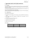
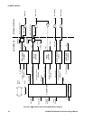
6.1.3 Architecture
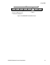
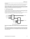
BSIO_SS[0]
BSIO_SS[1]
BSIO_DATA
BSIO_CLK
GP4020
BSIO
SERIAL
INTERFACE
CS
CS
CLK
CLK
DATA
DATA IN
EEPROM
LCD
DATA OUT
Figure 6.1 Using BµILD Serial Input Output (BSIO) with EEPROM and LCD peripherals
6.2 Operational Description
A control/status register configures the interface for each of the three select lines. A transfer register sets up
individual transfers with the number of words to write and read. A data register allows incoming data to be read
when in read mode and written when in write mode. An interrupt tells the ARM7TDMI when to read or write the data
register. If interrupts are disabled, the status register may be read to poll for when to read/write the data register.
The transfer register is used to initiate all transfers over the serial bus. Each write to the transfer register starts a
sequence of reads and writes over the bus directed by the data in the register. There are three possible scenarios
for transfers; write; read; write then read. In the read scenario after the transfer word is written, the chosen chip
select is asserted and data is read into the read buffer for the number of bytes required.
An interrupt is generated after each four bytes are read and at the end of the transfer to allow the ARM7TDMI to
read out the new word of data. Write mode works similarly where the data is written over the serial bus, with an
Interrupt occurring every four bytes of data. Write/Read mode starts with a number of bytes written over the
interface followed by a number of bytes read over the interface. A control bit allows for a one-cycle delay between
write and read for devices that require it. Write interrupts are generated during the write phase and then read
interrupts are generated during the read phase.
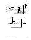
Example of a write of five bytes:
• The ARM7TDMI writes the first four bytes to the RWBUF register.
• The ARM7TDMI writes the control information to the transfer register.
• The Serial block copies the RWBUF register to an internal register and generates a write interrupt to the
ARM7TDMI to notify the RWBUF buffer is empty and begins sending data.
• The ARM7TDMI writes the last byte to the RWBUF register.
• The Serial block copies the RWBUF register to an internal register and generates a write interrupt to the
ARM7TDMI to notify the RWBUF buffer is empty and begins sending data once the first four bytes have been
sent.