


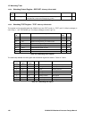
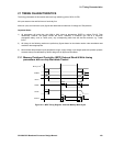
20: Input / Output pin Characteristics
188 GP4020 GPS Baseband Processor Design Manual
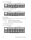
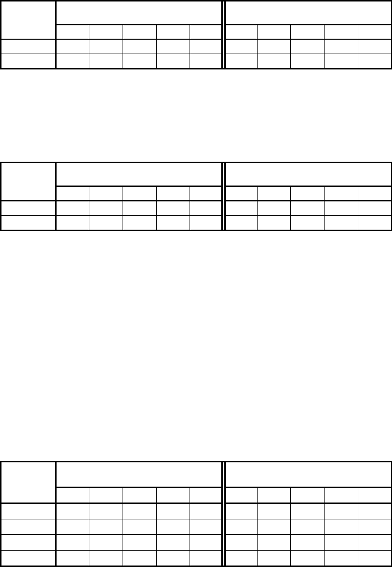
Input edge 0.1ns Input edge 1.5ns
Switching
Delay (ns)
Load
(fF)
Load
(fF)
50 100 250 500 1000 50 100 250 500 1000
IP → D ↑
0.29 0.34 0.49 0.74 1.23 0.40 0.45 0.60 0.84 1.34
IP → D ↓
0.29 0.31 0.39 0.51 0.76 0.62 0.64 0.72 0.84 1.09
Table 20.2 3.3V Input delays
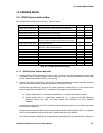
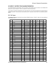
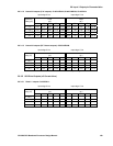
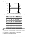
20.2.2 5V Tolerant Inputs: SCJIO1NR01N, SCJIP1NR
Switching characteristics at 25°C, 3.3V supply.
Input edge 0.1ns Input edge 1.5ns
Switching
Delay (ns)
Load
(fF)
Load
(fF)
50 100 200 400 800 50 100 200 400 800
IP → D ↑
0.31 0.36 0.47 0.68 1.11 0.38 0.44 0.54 0.76 1.18
IP → D ↓
0.58 0.60 0.65 0.74 0.93 0.85 0.87 0.92 1.01 1.20
Table 20.3 5V Tolerant Input delays
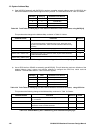
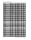
20.3 Output Delays
All delays quoted below are shown at midpoint temperature (+25°C), supply voltage (+3.3V) and silicon process for
all logic / data output lines in the GP4020.
Key: D → OP ↑ signifies Time from Data in going High, to Output going High
D → OP ↓ signifies Time from Data in going Low, to Output going Low
T → OP ↑ signifies Time from Tri-state Hi Impedance disable, to Output going High
T → OP ↓ signifies Time from Tri-state Hi Impedance disable, to Output going Low
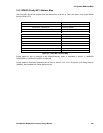
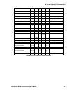
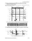
20.3.1 X01 Drive Outputs (x1 Current drive)
20.3.1.1 Slow L1 outputs: CLAOP01L1.
Input edge 0.1ns Input edge 1.5ns
Switching
Delay (ns)
Load
(pF)
Load
(pF)
10 20 40 80 150 10 20 40 80 150
D → OP ↑
6.03 7.72 10.36 14.03 18.74 5.75 7.45 10.09 13.76 18.47
D → OP ↓
8.09 9.52 11.73 14.75 18.56 8.90 10.33 12.54 15.57 19.38
T → OP ↑
6.32 8.02 10.67 14.38 19.16 7.13 8.83 11.49 15.19 19.97
T → OP ↓
8.09 9.51 11.71 14.72 18.52 8.89 10.32 12.52 15.53 19.33
Table 20.4 X01 Slow L1 3.3V Output delays