


7: 12-Channel Correlator
66 GP4020 GPS Baseband Processor Design Manual
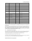
7.6.2 Tracking Channel Data Accumulation Registers
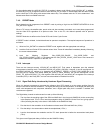
Each Tracking channel has the Data Accumulation registers as shown in Table 7.4 on page 67. Each address has
an independent read and write function. Complete address offset for each Channel Control register can be
determined using:
Correlator Register Address Offset =
CHx_Accumulate Base Address + Accumulate Register Offset
For Example, CH3_Q_TRACK = 0x240 + 0x004 = 0x244
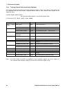
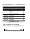
Address Offset Register Direction Function
CHx_
Control
+ 0x00 CODE_SLEW READ 11-bit Code Slew value
SATCNTL WRITE Configure C/A Code generator
+ 0x04 CODE_PHASE READ 11-bit Code Phase Count
CODE PHASE COUNTER
1
WRITE
Load Code Phase Counter
(test mode only)
+ 0x08 CARRIER_CYCLE_LOW READ 16 LSBs of Carrier Cycle Count
CARRIER_CYCLE_
COUNTER
1
WRITE
Load Carrier Cycle Counter
(test mode only)
+ 0x0C CARRIER_DCO_PHASE READ
10 MSBs of Carrier Phase Accumulator, sampled at
TIC
CARRIER_DCO_INCR_ HIGH WRITE 10 MSBs of Carrier DCO phase increment
+ 0x10 EPOCH (Latched) READ 1ms and 20ms EPOCH Counter values latched at last
TIC event.
CARRIER_DCO_INCR_ LOW WRITE 16 LSBs of Carrier DCO phase increment
+ 0x14 CODE_DCO_PHASE READ 10 MSBs of Code Phase Accumulator, sampled at TIC
CODE_DCO_INCR_HIGH WRITE 9 MSBs of Code DCO phase increment
+ 0x18 CARRIER_CYCLE_HIGH READ 4 MSBs of Carrier Cycle Count
CODE_DCO_INCR_LOW WRITE 16 LSBs of Code DCO phase increment
+ 0x1C EPOCH_CHECK (Not latched) READ Instantaneous values of 1ms and 20ms EPOCH
counters.
EPOCH_COUNT_LOAD WRITE 1ms and 20ms EPOCH Counter load values.
Table 7.3 CORR Tracking Channel Control Registers Map
Note 1: The CODE_PHASE_COUNTER and CARRIER_CYCLE_CONTROL registers can only be written to if
‘Test’ mode has been selected by setting bit 3 of the TEST CONTROL register to High.