


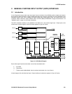

9: GPIO Interface
106 GP4020 GPS Baseband Processor Design Manual
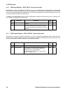
9.3.2 GPIO Input Register – GPIO_INPUT - Memory Offset 0x004
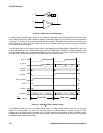
Readable only, a write to this address will produce a b_error. The instantaneous voltage condition on the external
pin is latched on each rising edge of ip_rd, which is synchronous with b_clk; and is available by a read from this
address. Any Output Register bits configured as OUT will have the respective data values echoed back via the I/O
pin, else the IN bits will read the external device.
In addition, if the echoed back value of an OUT-configured bit is different to the data value, this is evidence of an
error, possibly an external output-driver clash.
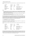
Bit
No.
Mnemonic Description
Reset
Value
R/W
31: 8 -
Reserved
--
7:0
GPIO_INPUT[7:0]
GPIO Input. Each GPIO_INPUT bit maps to a single
GPIO pin and allows the value of the pin to be read.
(i.e. GPIO_INPUT[4] maps to GPIO[4] (pin 95 (100-pin
package)))
-R
Table 9.4 GPIO_INPUT Register
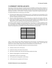
9.3.3 GPIO Output Register – GPIO_OUTPUT - Memory Offset 0x008
Writeable only, a read to this address will produce a b_error. A write to this register stores logic values which are
driven to the pins when enabled by an OUT in the corresponding DIRECTION REGISTER bit. When direction is IN
the logic value will have no effect, although it is still stored in the latch.
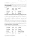
Bit
No.
Mnemonic Description
Reset
Value
R/W
31: 8 -
Reserved
--
7:0
GPIO_OUTPUT
GPIO Output. Each GPIO_OUTPUT bit maps to a
single GPIO pin. (i.e. GPIO_OUTPUT[4] maps to
GPIO[4] (pin 95 (100-pin package))).
When configured as an output, a "1" drives a High
output, a "0" drives a Low.
0x00 W
Table 9.5 GPIO_OUTPUT Register