


14: System Clock Generator
138 GP4020 GPS Baseband Processor Design Manual
Z
o
= Output Impedance of oscillator at PRX_OUT
G
m
= Transconductance of oscillator
R
f
= Feedback Resistor (on-chip)
ESR = Equivalent Series Resistance of crystal
F = Fundamental Crystal frequency
Equations 1 and 2 above can be used to calculate the range of tolerable crystal capacitance values, when the
crystal characteristics are known (frequency and ESR). Typical values for C1 and C2 for a 10.0MHz crystal will be
47pF each, and for a 16.0MHz crystal will be 39pF each. This assumes a crystal ESR of approx. 25Ω, output
impedance of 110kohms and an oscillator transconductance of 2.24mA/V.
The capacitor values used with the Processor Crystal Oscillator are NOT critical, and calculations of values will not
normally be required. However, some crystals may have some exceptional ESR values, or more appropriately, the
range of oscillator coefficients over all environmental conditions may be a concern.
14.3.1 Using the Processor Clock Oscillator with an external frequency source
Some GPS receiver systems may use an external oscillator (TCXO) to generate a PLL reference for the RF Front-
end device. There may be instances where the Processor Clock Oscillator may need to be used when the RF
Front-end is powered down, and the cost of an additional crystal for the GP4020 is deemed an unacceptable extra
expense.
The PRX_IN (pin 66 (100-pin package)) input to the processor Clock oscillator is NOT a true CMOS input, due in
part to the on-chip feedback resistor that is used with the oscillator itself. Because of this, the PRX_IN input has a
high input capacitance (approx. 20pF), which will mean that the input impedance will be low at a frequency of
10MHz (approx. 800ohms). Hence, the drive from the TCXO will need to be low-impedance to ensure that
adequate signal triggers the Processor Clock buffer.
The GP4020 presents a noisy load to any analogue signals connected to it. As the TCXO drives the RF Front-end
PLL, it is imperative to ensure that the RF PLL does not get interference via the TCXO from the GP4020. The GPS
system performance can be severely degraded if the RF Front-end cannot produce an accurate set of Local-
Oscillator signals for the IF down-conversions. Therefore, it is important to ensure that the quality of the TCXO is
NOT degraded by the GP4020.
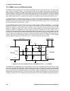
Consequently, it is recommended that if the TCXO is going to be used to provide a backup system clock while an
RF Front-end is powered down, that some active buffering be introduced between the TCXO and the GP4020
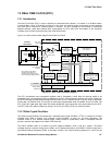
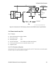
PRX_IN input. Figure 14.4 below shows the generic connection scheme of a TCXO to both a GPS RF Front-end
(e.g. GP2015), the GP4020, and a recommended TCXO buffer circuit, using a CMOS inverter gate. The gate uses
a feedback resistor in order to bias the gate input to be approx. mid-rail (1.65V DC) when no external signal is
driving it. Note that the TCXO uses a supply resistor and some large capacitors to assist with Power Supply
Rejection, particularly from digital interference on the power-supply at low frequencies.
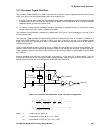
The TCXO buffer circuit is a biased high-speed CMOS logic gate. As the gain of a Logic Gate is VERY high, the
output from it is essentially a square-wave, which gives a very good drive signal for the GP4020. This results in a
low-jitter BµILD_CLK signal. It is very important to ensure that the Logic Gate is powered from the same PSU line
as the TCXO, in order to offer the highest degree of buffering between TCXO and GP4020.It may be appropriate to
use a single-gate Logic chip for the TCXO buffer. Many logic gates are now available not only in quantities of 4 or 6
in a standard 14-pin package, but also as single gates in SOT-23 style packages.
Care should be used to minimise the effects of radiated 10MHz harmonics when using a TCXO buffer. Many
buffers have bandwidths well into 100s of MHz. Poor layout of tracks from this buffer in a GPS Receiver could
produce radiated interference at harmonics of 10MHz. This could affect the GPS RF Front-end sensitivity, and
create EMC problems. It may be necessary to introduce a series resistor (approx. 33Ω or more) between the TCXO
buffer output and the PRX_IN pin on the GP4020, to reduce the harmonic energy from the TCXO Buffer.