


4: Boot ROM
GP4020 GPS Baseband Processor Design Manual 27
4 BOOT ROM
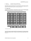
4.1 Functional Description
The GP4020 Boot ROM is an internal part of the IC. The code in the Boot ROM will allow the GP4020 based GPS
receiver to up-load a software routine into RAM from an external data source (e.g. a PC), and run the routine from
RAM. The uploaded routine could be used to update the GPS application firmware stored in FLASH EPROM. The
Boot ROM does NOT need to run every time the GP4020 is powered up. There are a number of methods used to
select either the internal Boot ROM or an External ROM.
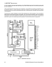
The Boot ROM contains code that executes from address 0x0000 0000 via Firefly address area select line NCS[0].
The GP4020 can be configured to use either the internal ROM for system boot-up or an external ROM. This can be
influenced by whether the GP4020 based GPS receiver is:
a) running final application software which can boot from an external ROM;
b) running a software utility is downloaded via UART1, booted using the internal ROM.
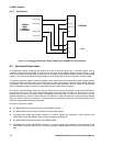
The GP4020 contains two mechanisms to select whether the NCS[0] signal from the Firefly MPC addresses the
internal boot-ROM, or an external device connected to NSCS[0] (pin 11 (100-pin package)):
1) Control bit EXT_NCS0 in the IO_REV register within the PCL block.
2) A Latch that stores the state of MULTI_FNIO (pin 54 (100-pin package)) at the end of a chip reset due to
the NPOR_RESET signal. Refer to Section 12.2 "Chip Reset Logic" on page 113 for details on this reset
mechanism.
Setting EXT_NCS[0] (bit 9 of the IO_REV register) can disable the Boot ROM. However, if MULTI_FNIO is low
during a reset of the Firefly MF1 core, this control bit has no effect; it cannot override the hardware disable.
The Boot ROM is a maximum size of 512 words (16-bits wide). The code execution is dependent upon the input
value on the MULTI_FNIO pin. This pin is by default set to be an input, although this can be re-configured with
application software by the Peripheral Control Logic, after the Boot Code has run.
A reset due to NSRESET (pin 75 (100-pin package)) going Low, or a Watchdog time-out, will cause the internal
signal NPOR_RESET to be active (low).
NPOR_RESET will cause the EXT_NCS0 bit in the IO_REV register to be cleared.
In addition, at the rising edge of NPOR_RESET, the state of MULTI_FNIO is latched. The latched version of
MULTI_FNIO is inverted, to generate a signal called INT_NCS[0].
If INT_NCS[0] is high (i.e. MULTI_FNIO (pin 54 (100-pin package)) was low at rising edge of NPOR_RESET) OR
EXT_NCS0 is high, then NCS[0] from Firefly selects external NSCS[0] ROM device. Otherwise, the internal boot-
ROM is selected.
A Read of the EXT_NCS0 bit in the PCL IO_REV register, will return the actual NCS[0] source selected (i.e. If
INT_NCS[0] is high, EXT_NCS0 bit will always be read as '1', irrespective of what is written to it. If INT_NCS[0] has
been used to select the external NSCS[0], the EXT_NCS0 bit cannot be used to switch back to using internal boot-
ROM).
If the internal boot-ROM is selected, when the Firefly reset is released, it will:
1) Download data from UART1 and store it in internal RAM (using the protocol defined below);
2) Use an MPC function (configured in the SSM System Configuration Register) which swaps the address ranges
of the Firefly Memory area Select lines, NCS[0] and NCS[3]. (i.e. the internal boot-ROM and NSCS[0], with the
Internal RAM space). This effectively swaps the memory space of the internal SRAM (0x6000 0000), with the
space for the Internal Boot ROM (0x0000 0000). The internal SRAM space then effectively starts from 0x0000