


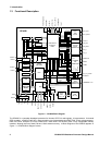
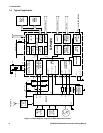

1: Introduction
GP4020 GPS Baseband Processor Design Manual 5
1.3.9 General Purpose Input Output (GPIO)
This module provides eight I/O pins, which may be bit or byte addressed and configured in a latched or transparent
mode. When in byte mode, buffer full/empty flags are available which can be used to generate an interrupt to the
ARM7TDMI processor.
Details can be found in section 9 "GENERAL PURPOSE INPUT OUTPUT (GPIO) INTERFACE" on page 103.
1.3.10 Interrupt Controller (INTC)
The ARM7TDMI core accepts two types of interrupt: Normal (IRQ) and Fast (FIQ). All Interrupts can be switched
between types, depending upon the relative priorities required.
The INTC is the central control logic that decodes the priority level and handles interrupt request signals from a
number of external sources.
Details can be found in section 10 "INTERRUPT CONTROLLER (INTC)" on page 107.
1.3.11 Memory/Peripheral Controller (MPC)
The MPC ensures the correct multiplexing of data is applied for bus transfers between 8-, 16- or 32-bit on-chip
macrocells, and 8- 0r 16-bit off-chip peripherals. Four different contiguous memory areas are available, each with
an address range of one MByte, with individually programmable wait- and stop-state generation. A “SWAP” function
allows memory area “1”, which is addressed at system reset, to be switched with memory area “4”. This allows, for
example, booting from ROM and then switching memory area 1 to address SRAM so that time-critical software and
interrupt routines can operate from fast memory.
Details can be found in section 11 "MEMORY PERIPHERAL CONTROLLER (MPC)" on page 109.
1.3.12 Peripheral Control Logic (PCL)
The GP4020 incorporates some specific control logic, which is used to control a number of functions:
• System Reset Control
• System Power-down, Sleep and Wake-up Control
• System Status and Control Registers
• Signal input/output multiplex control
Details can be found in section 12 "PERIPHERAL CONTROL LOGIC (PCL)" on page 113.
1.3.13 Internal SRAM
The GP4020 contains 8k bytes (configured as 2k x 32-bit) of high-speed (6ns) Static RAM. This can be used for
either:
• Non-volatile storage of GPS data (Almanac, Ephemeris, Position and Receiver Clock Offset), while the
receiver power is disabled.
• A High-speed Interrupt Service Routine, while the GP4020 is powered up.
The internal SRAM appears at GP4020 Base Address 0x6000 0000, served by the MPC Memory Area 4. An MPC
SWAP function can swap this memory space with 0x0000 0000 if required.