


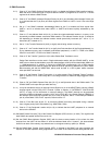

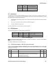

9: GPIO Interface
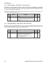
104 GP4020 GPS Baseband Processor Design Manual
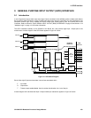
1N
F
D
T
IO
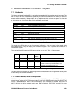
Figure 9.2 GPIO Pad Cell Configuration
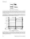
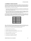
The GPIO module must be read or written in 32-bit accesses, although only the lower eight bits of the BµILD data
bus (b_data[7:0]) are used. Data is written to registers on the falling edge of B_CLK. Data is read from registers on
a high (logic '1') value of B_CLK (see diagram BµILD Bus Interface). During the read operation the remaining 24-
bits of the 32-bit bus are not driven, and will be held to a non-floating value by the bus hold cells (a chip-wide
resource external to this module).
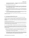
The nCS signal goes low if a memory access occurs in the address range 0xE000 5000 to 0xE000 5FFF, that is the
I/O area allocated to the GIO. The bus decoding only tests B_ADDR[3] and B_ADDR[2], so multiple reflection of the
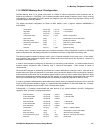
four valid (three actually used ) 32-bit address spaces will occur over this range. Figure 9.3 below shows the timing
of the BµILD Bus interface to the GPIO for both Data Read and Data Write cycles.
B_CLK
B_DATA
B_ADDR
& B_SIZE
B_WRITE
SLEEP_CLKEN
Read Cycle Write Cycle
B_WAIT
B_ERROR
Valid
Z Z Z Z Z
Z
note.
Z = high impedance
nCS
ValidBus hold
Driven DrivenBus holdBus hold
Figure 9.3 GPIO BµILD Bus interface timing
The B_ERROR signal goes high if an illegal access occurs. An illegal access means a read from a write only
register or unused location, or a write to a read only register or unused location. In addition, if 8-bit or 16-bit
accesses occur B_ERROR will be asserted, this is to assist software error checking. Whilst B_ERROR is being
asserted data writes are disabled and will not modify registers, but read operations will still drive the bus with data if
a readable register exists at that location.