


19: System Address Map
GP4020 GPS Baseband Processor Design Manual 181
19 ADDRESS MAPS
19.1 GP4020 System Address Map
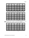
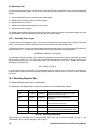
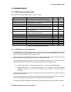
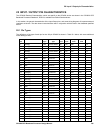
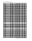
The GP4020 has the Address Map as shown in Table 19.1 below.
ADDRESS RANGE FUNCTION MPC Area NOTES
0x0000 0000 - 0x000F FFFF Internal Boot ROM or External Boot ROM via NSCS[0] 1 1
0x0010 0000 - 0x1FFF FFFF
Not Used (Int./Ext. Boot ROM reflected)
0x2000 0000 - 0x200F FFFF External Chip Select 1 via NSCS[1] 2
0x2010 0000 - 0x3FFF FFFF
Not Used (CS1 reflected)
0x4000 0000 - 0x400F FFFF External Chip Select 2A via NSCS[2A]
NOTE: Correlator, Peripherals REFLECTED every 0x2000
32
0x4010 0000 - 0x4010 0FFF 12-Channel Correlator 3 2
0x4010 1000 - 0x4010 1FFF Peripheral Control Logic, Real Time Clock, System Clock
Generator, 1PPS Timemark Generator
32
0x4010 2000 - 0x5FFF FFFF
Not Used (CS2, Correlator, Peripherals reflected)
0x6000 0000 - 0x6000 1FFF Internal SRAM - 2k x 32-bit 4
0x6000 2000 - 0x7FFF FFFF
Not Used (CS3 reflected)
0x8000 0000 - 0xDFFF FFFF
Reserved
0xE000 0000 - 0xE00F FFFF
Firefly MF1 B
µILD bus modules
0xE010 0000 - 0xFFFF FFFF
Reserved
Table 19.1 GP4020 System Address Map
19.1.1 GP4020 System Address Map Notes
1) Internal or External ROM is selected by the state of MULTI_FNIO (pin 54 (100-pin package)) during chip reset
via NSRESET (pin 75 (100-pin package)) Low or Watchdog time-out. External ROM selected if MULTI_FNIO
set low. Internal ROM selected by MULTI_FNIO set High.
2) External Chip Select 2A (NSCS[2A]), the internal 12-channel correlator and GP4020 Peripherals share the
same wait-state characteristics as defined within Memory Peripheral Controller.
The NSCS[2A] chip-select line is active for ALL memory accesses in Memory Area 3 (i.e. ALL memory space
between 0x4000 0000 and 0x5FFF FFFF, including the internal logic blocks as defined below:
• (System Address Bit 20 = 1 AND System Address Bit 12 = 0) selects the GP4020 Correlator.
• (System Address Bit 20 = 1 AND System Address Bit 12 = 1) selects the GP4020 Peripherals
(Peripheral Control Logic, Real Time Clock, System Clock Generator, and 1PPS Timemark
Generator).
An access to an external area WILL NOT be reflected into the internal logic blocks, but an internal area access
WILL be reflected externally.
What this means is that the Address Space occupied between 0x4010 0000 and 0x4010 1FFF (i.e. 0x0000 to
0x1FFF) will be reflected through the whole Area 3 Address space once every 0x2000.
The limitation indicated in NSCS[2A] can be bypassed by undertaking either of the following fixes in Hardware: