


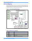
Chapter 6 Memory Map and Registers
ATCA-C110/1G Installation and Use Manual
75
REVIEW COPY
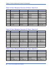
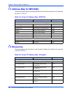
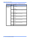
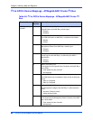
Temperature Sensor Board Temperature Sensor,
LM75CIM
0x9E
FIM Devices
BIB - EEPROM for Fabric Interface
Module
Board Information Block EEPROM 0xAE
I
2
C to GPIO Device HotPlug control
PCA9557PW
0x32
I
2
C ADC Onboard ADC, AD7997 0x41
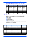
Table 6-5. Private I
2
C Address Map - ATmega8L (continued)
Device Device description Address
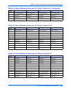
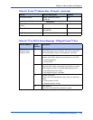
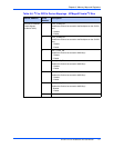
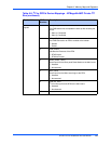
Table 6-6. I
2
C to GPIO’s Device Mappings - ATMega8 Private I
2
C Bus
Device Address GPIO
Number
Description
Telecom Clock
Selection Device
(Address: 0x38)
0:2 CLKSEL[0:2]
Selects the Clock source to the DPLL, the clock source can be
from the AMC Bay3 or Bay4 or the Backplane or the RTM.
3 SYNC_RTM_OR_BPLANE
Selection of the SYNC Signal from the backplane or the RTM
0 - From the Backplane
1 - From the RTM
4 CLK1_SEC_OR_SYNC
Selects the CLK1 buffer input selection signal either it is 8 kHz
Frame Alignment Clock or 19.44 MHz Byte Alignment Clock
0 - Frame Alignment Clock, 8 kHz
1 - Byte Alignment Clock, 19.44 MHz
5 BPLANE_CLK3_SEL
Selection of the ATCA Backplane Clock, primary or secondary
source
0 - Primary Source, CLK3A
1 - Secondary Source, CLK3B
6:7 CLK3_SEL[0:1]
Netref Clock (CLK3) buffer input selection signals