


6
ATCA-C110/1G Installation and Use Manual
71
REVIEW COPY
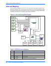
6 Memory Map and Registers
This chapter describes the following mapping information for the ATCA-C110/1G board:
■ Memory Maps on page 71
■ Interrupt Mapping on page 72
■ Shelf Management Registers (IPMI interface) on page 73
■ I2C Address Map for MPC8540 on page 74
■ I2C Resources on page 74
■ GPIO on page 82
■ Ethernet Phy Address Map on page 82
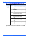
Memory Maps
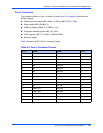
The following table shows the ATCA-C110/1G’s main address map.
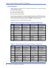
The CS# mapping is listed in the table below.
The I/O addresses of all onboard functional units are listed below.
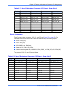
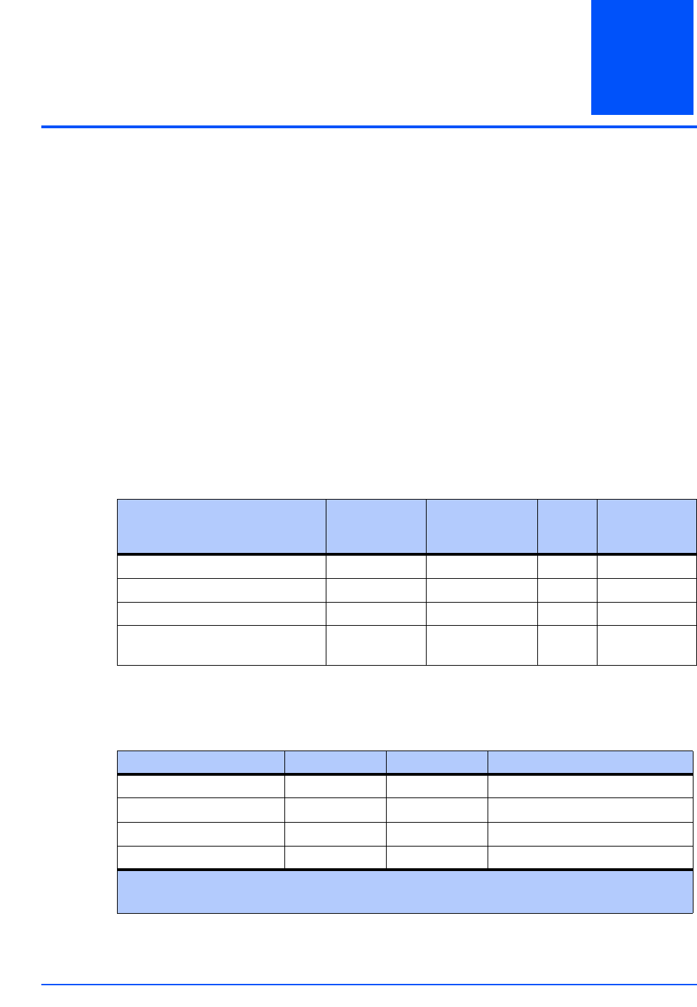
Table 6-1. Memory Address Map
Memory Base Address
Device
Configuration
Data
bus
width
Chip Select
2 MB Primary Boot Flash FFE00000 16 Mbit Device 8 CS0
2 MB Secondary Boot Flash FFE00000 16 Mbit Device 8 CS0
SDRAM base address 00000000 512 Mbit Device 64 CS0 to CS3
MPC8540 control, configuration,
status registers base address
C0000000 NA NA NA
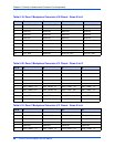
Table 6-2. CS# Mapping of Main Memory on ATCA-C110/1G
PowerQUICC III Signal Physical Bank Rank Signal on DIMM/Device
MCS0# Bank 1 Rank 0 CS0#
MCS1# Bank 1 Rank 1 CS1#
MCS2# Bank 2 Rank 0 CS2#
MCS3# Bank 2 Rank 1 CS3#
Bank1 refers to the onboard memory and Bank 2 to the SODIMM memory. The Rank 1 refers
to the stacked memory on each physical bank.