


ATCA-C110/1G Installation and Use Manual
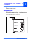
Chapter 5 Controls, Indicators and Connector Pin Assignments
54
REVIEW COPY
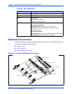
The four FIM connectors: J1, J2, J3 and J4, onboard the ATCA-C110/1G are described below.
See Figure 5-2 on page 52 for location of FIM connectors.
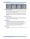
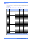
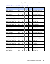
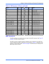
26 PICMG3.1, Fabric
Interface
Gig SerDes Port 0 2 BCM56502
27 Gig SerDes Port 1 2 BCM56502
28 Gig SerDes Port 2 2 BCM56502
29 Gig SerDes Port 3 2 BCM56502
30 Gig SerDes Port 4 2 BCM56502
31 Gig SerDes Port 5 2 BCM56502
32 Gig SerDes Port 6 2 BCM56502
33 Gig SerDes Port 7 2 BCM56502
34 RTM Gig SerDes
Port 0
2 BCM56502
35 Gig SerDes
Port 1
2 BCM56502
36 Gig SerDes
Port 2
2 BCM56502
37 Gig SerDes
Port 3
2 BCM56502
38 XAUI Link 8 BCM56502
39 Update port XAUI Link 8 BCM56502
40 Reference Clock PCI-Express 2 ICS9DB102
TOTAL 122 differential pairs
Table 5-2. Differential Signals between FIM and Baseboard (continued)
Pin # Group Link No. of
differential
pairs
Device on FIM
The four FIM connectors provide a total of 144 differential pairs. The unused pins are
used for Power, JTAG, Reset and Control signals.
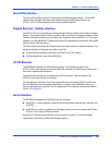
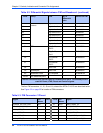
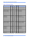
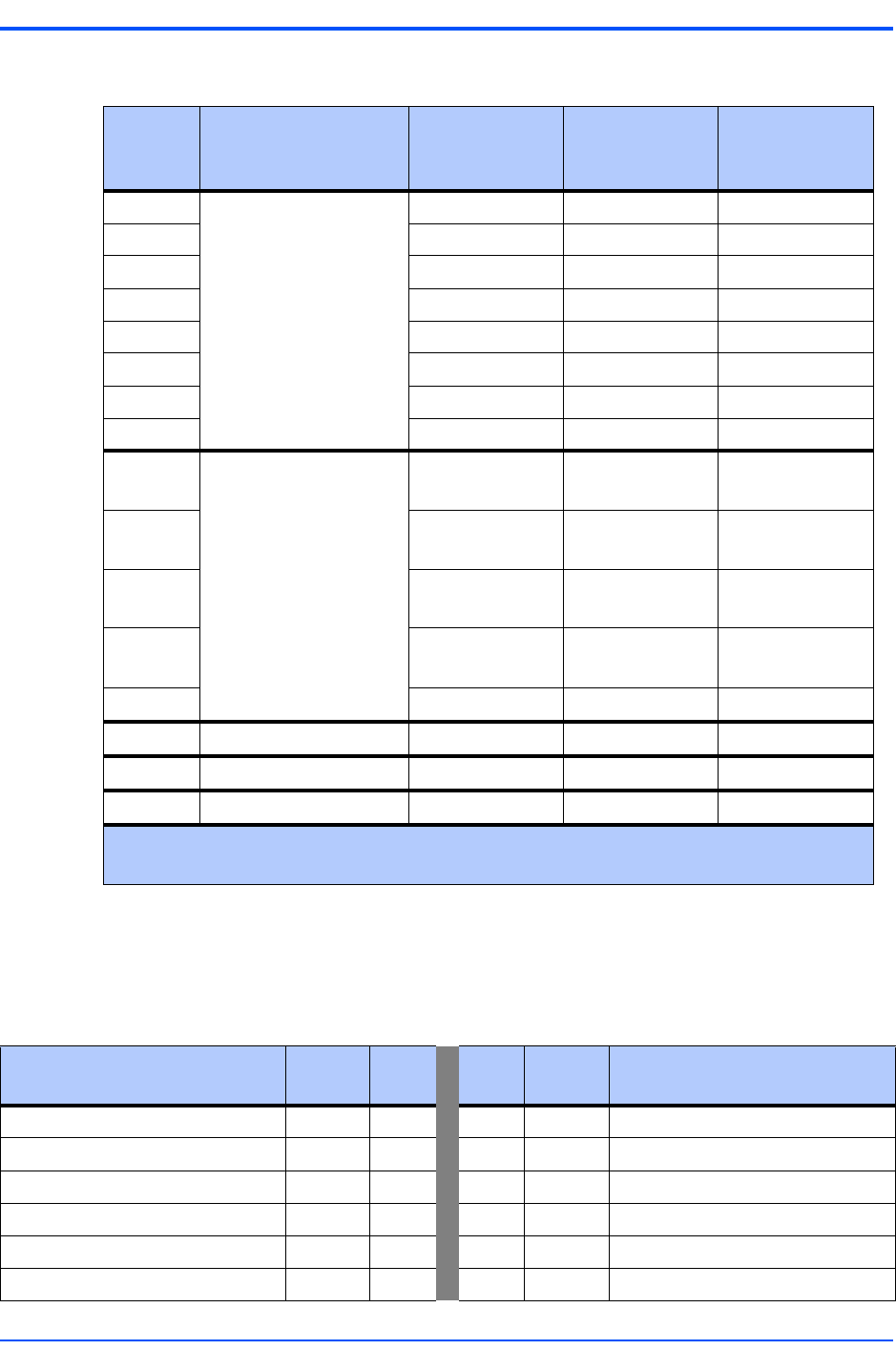
Table 5-3. FIM Connector J1 Pinout
Signal Pin
Name
Pin # Pin # Pin
Name
Signal
PEX8532_PCI_EXP_CLK+ S1+ 1 37 S19+ AMC3_SATA0_TX+
PEX8532_PCI_EXP_CLK- S1- 2
38 S19- AMC3_SATA0_TX-
AMC4_GBE0_TX+ S2+ 3
39 S20+ AMC3_SATA1_TX+
AMC4_GBE0_TX- S2- 4
40 S20- AMC3_SATA1_TX-
AMC4_GBE1_TX+ S3+ 5
41 S21+ AMC4_PCIEXP_LANE0_TX+
AMC4_GBE1_TX- S3- 6
42 S21- AMC4_PCIEXP_LANE0_TX-