


4
ATCA-C110/1G Installation and Use Manual
35
REVIEW COPY
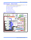
4 Functional Description
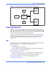
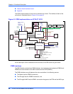
This chapter describes the functional concepts of the ATCA-C110/1G as well as the main
physical and electrical structure of the board.
ATCA-C110/1G Overview
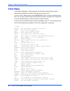
The following table lists the features of the ATCA-C110/1G.
Table 4-1. ATCA-C110/1G Overview
Feature Description
Service Processor and Interfaces
Processor MPC8540 at 833 MHz core frequency utilizing a SoC platform
Memory Devices
Main Memory Default memory capacity:
Onboard - 512 MB
SODIMM - 512 MB
Boot Flash Boot Flash Memory (with the Recover Image) of size 2 MB for Firmware Image
User Flash User Flash Memory of size 128 MB
Modules
FIM Fabric Interface Module (FIM), which performs switching functions for fabric links
Features a 24-port GbE switch, a PCI-Express switch and a SATA Multiplexer
AMC Bays Upto four AMC Bays, B+ single width type
ARTM Rear Transition Module to route the I/O interface from the carrier and the FIM
board out of the system
I/O interfaces
PCI-Express One x4 PCI-Express link routed to each AMC Bay
One x4 link through a PCI-to-PCI-Express bridge routed to the Service Processor
Ethernet Support for Base and Fabric Interface of PICMG 3.0 and PICMG 3.1
Two SerDes interfaces routed from FIM to each AMC Bay
Two GbE interfaces of the Processor routed to the FIM
Four SerDes interfaces routed from FIM to the RTM (Zone 3)
One XAUI interface routed from FIM to the RTM (Zone 3)
One 10/100 interface routed from the Processor to the RTM (ATCA Zone 3)
Serial One UART Port from the Processor to the RTM
One UART Port from the Processor to the IPMC as the Payload interface
SATA Two SATA links from each AMC Bay to FIM