


ATCA-C110/1G Installation and Use Manual
Chapter 4 Functional Description
40
REVIEW COPY
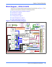
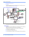
PCI/PCI-X Interface
The MPC8540 provides PCI/PCI-X interface that complies with the PCI Local Bus Specification,
Rev. 2.2 and the PCI-X Addendum to the PCI Local Bus Specification, Rev. 1.0a.
The PCI interface is 64-bit wide and runs at 66 MHz and is the interface between the MPC8540
and the PEX8114 PCI/PCI-X to PCI-Express Bridge.
Main Memory
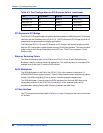
The main memory on ATCA-C110/1G has two physical banks: Onboard Memory and SODIMM.
The onboard memory has a capacity of 512 MB and uses 512 Mbit devices. The SODIMM slot
can use either single-rank or dual-rank modules. The chip select mappings of main memory is
shown in Table 6-2 on page 71.
ATCA-C110/1G supports single channel unbuffered, onboard, first generation DDR memory of
capacity 1 GB. The base operating frequency of the DDR memory is 166 MHz, with peak data
rate of 333 MHz. The data bus width of the memory controller is 64-bit (8 bytes) with 8-bit ECC.
Onboard Memory
The onboard memory bank of the ATCA-C110/1G consists of nine 512 Mb devices, eight for
data storage and one for ECC. It supports a CAS Latency of 2.5 Clock cycles.
The onboard memory is unbuffered. An I
2
C compatible SPD EEPROM chip contains
information of the onboard memory on the I
2
C interface of the MPC8540. Stacking on onboard
memory is supported.
SODIMM
The ATCA-C110/1G supports ECC-enabled unbuffered SODIMM memory on the second
Physical bank of the main memory. The SODIMMs may be single or dual ranked.
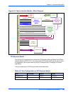
Boot Device
The boot device on the ATCA-C110/1G is a 2 MB Primary Boot Flash located on the GPCM
interface of the MPC8540. The ATCA-C110/1G also provides one redundant (Secondary) 2 MB
Boot Flash device.
Note If the Primary Boot Flash fails, the IPMC enables the Secondary Boot Flash device.
Figure 4-2 on page 41 shows the connections made to the Primary and Secondary Boot Flash.