


Page B-18 400 SERIES MAINTENANCE MANUAL
Rev. C P/N 190-00140-05
B.11 DISPLAY MODULE CONNECTORS
B.11.1 J22
See LCD Flex description (J12).
B.12 DATA BASE CARD CONNECTORS
J20 and J21 are the Data Base Card Connectors.
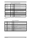
B.13 MAP BOARD CONNECTORS
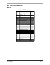
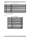
B.13.1 P16
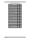
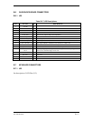
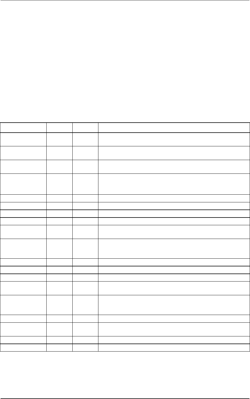
Table B-22. P16 Descriptions
Pin Name Pin # I/O DESCRIPTION
CS_MAPN 1 O Chip Select Map Not. Output pulses low typically for 240 ns when
map is accessed.
RDN 2 O Read Not. Output pulses low for typical times of 90, 150, and 210
ns, depending on wait states.
WRN 3 O Write Not. Output pulses low for typical times of 60, 120, and 180 ns,
depending on wait states.
CCSR0N_MCS0N
..
CCSR3N_MCS3N
4..7 O Card Chip Select Right 0..3 not and Map Chip Select 0..3. Signal
used for both card chips (only 1 should be low at a time) and selecting
map.
SPARE 8, 10, 54
RESETN 9 O Reset Not output. Low when resetting.
D00 to D15 11..26 B1 Data I/O.
A01..A13 27..39 O Address 01.. 13 output.
CMA14..CMA23 40..49 O Card and Map Address output. Used for both addressing map and
card data.
CCSL0N_MA24..
CCSL3N_MA27
50..53 O Card Chip Select Left 0..3 not and Map Address 24..27. Used for
chip selects of left card (only 1 of 4 should be low at a time) and
addressing map data.
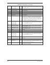
12V_REG 55 O 12 V dc +/- 5% output.
VCC 56 O
GND 57 O Ground.
M_CFG3..M_CFG
0
58..61 I Map Configuration Input 3..0.
WR_TESTN 62 O Write Test Not. Output pulses low for typical times of 60, 120, and
180 ns, depending on wait states and only if the J1-76 (TEST MODE
SELECT) is low. Also see J14-46 (LFT_A22).
SPARE 63..66
HSBUS_A,
HSBUS_B
67, 68 I/O Not used.
UXLA01 69 O Uart, Xilinx, LCD Address 1.
HSBUS_RESETN 70 O Not used.