


Page B-14 400 SERIES MAINTENANCE MANUAL
Rev. C P/N 190-00140-05
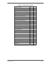
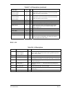
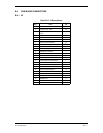
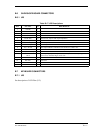
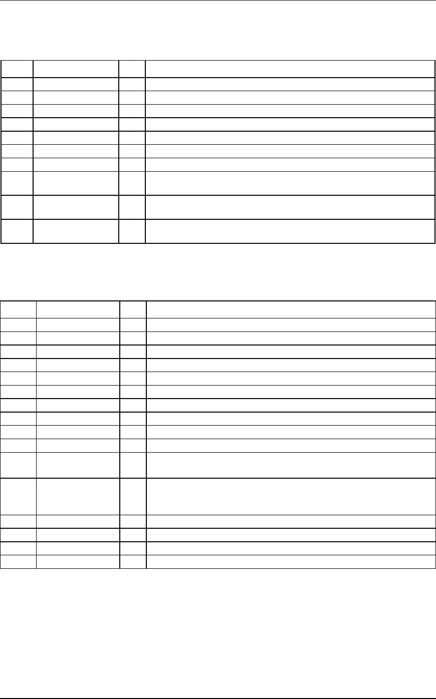
B.5.2 J10
Table B-15. J10 Descriptions
Pin # Pin Name I/O Description
1 +12VDC I
2 +5VDC I
3 GND I
4 -12VDC I
5 VLOC SERIAL IN I Serial input from the Main CPU board to the NAV Board.
6 KEY - This pin is not used.
7 G/S SERIAL IN I Serial input from the Main CPU board to the G/S board.
8 G/S SERIAL OUT O This is an asynchronous serial output from the G/S board to the Main CPU
board.
9 NAV VOL
CONTROL
I This is a dc input in the range between 0 and 5 volts coming through the
Main CPU board from the NAV volume control pot mounted on the bezel.
10 VLOC SERIAL
OUT
O This is a asynchronous serial output to the Main CPU board from the NAV
Board.
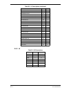
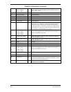
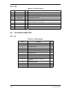
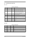
B.5.3 J24
Table B-16. J24 Descriptions
Pin # Pin Name I/O Description
1 +12VDC O
2 +5VDC O
3 GND O Ground.
4 -12VDC O
5 G/S IF AGC I Glideslope board IF AGC output.
6 NOT USED I
7 G/S SERIAL IN O Serial output to the G/S board from Main Board.
8 G/S SERIAL OUT I Serial input from the G/S board to the Main Board
9 G/S + FLAG I Input from the G/S board.
10 G/S + UP I Input from the G/S board.
11 G/S -
[COMMON]
I The G/S board COMMON, or G/S -, input. Reference for the G/S + UP and
G/S + FLAG.
12 G/S
SUPER FLAG
OUT
I G/S board superflag input. (Output on the G/S board is an open collector
output. The G/S superflag will be active (low) when the flag is out of view.)
13 KEY -
14 G/S RF AGC I Not Used.
15 SPARE - SPARE
16 KEY -