


400 SERIES MAINTENANCE MANUAL Page B-9
P/N 190-00140-05 Rev. C
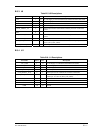
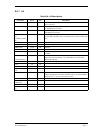
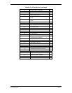
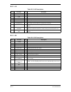
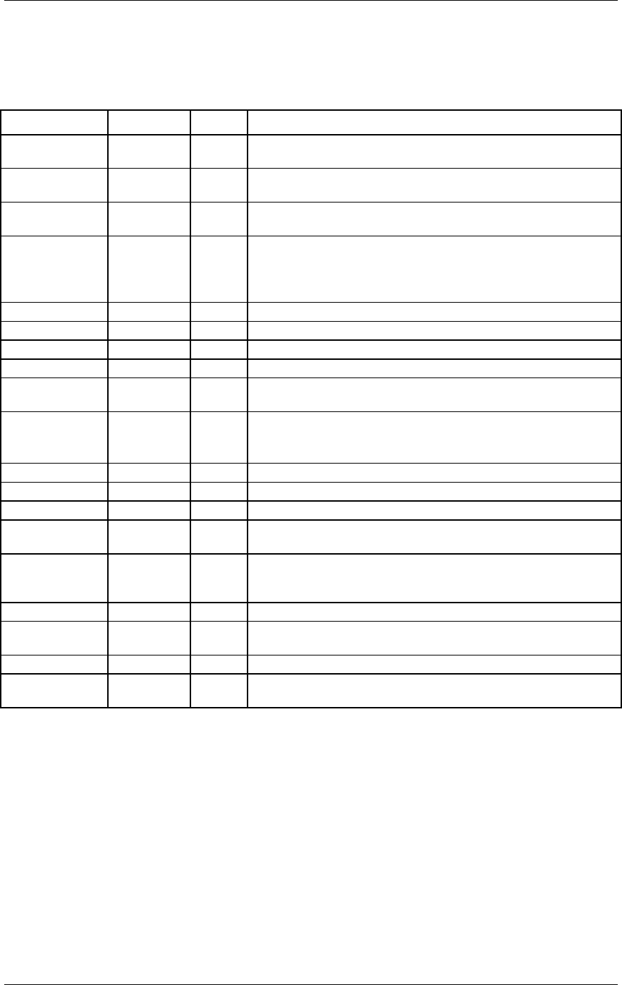
B.3.7 J16
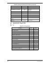
Table B-9. J16 Descriptions
Pin Name Pin # I/O Description
CS_MAPN 1 O Chip Select Map Not. Output pulses low typically for 240 ns when
map is accessed.
RDN 2 O Read Not. Output pulses low for typical times of 90, 150, and 210
ns, depending on wait states.
WRN 3 O Write Not. Output pulses low for typical times of 60, 120, and 180 ns,
depending on wait states.
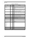
CCSR0N_MCS0
N..
CCSR3N_MCS3
N
4..7 O Card Chip Select Right 0..3, not and Map Chip Select 0..3. Signal
used for both card chips (only 1 should be low at a time) and selecting
map.
SPARE 8, 10, 54
RESETN 9 O Reset Not output. Low when resetting.
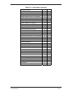
D00 to D15 11..26 B1 Data I/O.
A01..A13 27..39 O Address 01.. 13 output.
CMA14..CMA23 40..49 O Card and Map Address output. Used for both addressing map and
card data.
CCSL0N_MA24.
.
CCSL3N_MA27
50..53 O Card Chip Select Left 0..3 not and Map Address 24..27. Used for
chip selects of left card (only 1 of 4 should be low at a time) and
addressing map data.
12V_REG 55 O 12 V dc +/- 5% output.
VCC 56 O
GND 57 O Ground.
M_CFG3..M_CF
G0
58..61 I Map Configuration Input 3..0.
WR_TESTN 62 O Write Test Not. Output pulses low for typical times of 60, 120, and
180 ns, depending on wait states and only if the J1-76 (TEST MODE
SELECT) is low. Also see J14-46 (LFT_A22)
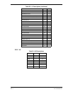
SPARE 63..66
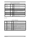
HSBUS_A,
HSBUS_B
67, 68 I/O Not used.
UXLA01 69 O Uart, Xilinx, LCD Address 1.
HSBUS_RESET
N
70 O Not used.