


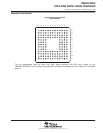

TMS320VC5402
FIXEDĆPOINT DIGITAL SIGNAL PROCESSOR
SPRS079E – OCTOBER 1998 – REVISED AUGUST 2000
9
POST OFFICE BOX 1443 • HOUSTON, TEXAS 77251–1443
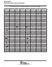
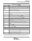
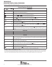
Terminal Functions (Continued)
TERMINAL
NAME
DESCRIPTIONTYPE
†
TERMINAL
NAME
DESCRIPTIONTYPE
†
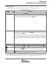
OSCILLATOR/TIMER SIGNALS
CLKOUT O/Z
Master clock output signal. CLKOUT cycles at the machine-cycle rate of the CPU. The internal machine cycle
is bounded by rising edges of this signal. CLKOUT also goes into the high-impedance state when OFF
is low.
CLKMD1
CLKMD2
CLKMD3
I
Clock mode select signals. These inputs select the mode that the clock generator is initialized to after reset. The
logic levels of CLKMD1–CLKMD3 are latched when the reset pin is low, and the clock mode register is initialized
to the selected mode. After reset, the clock mode can be changed through software, but the clock mode select
signals have no effect until the device is reset again.
X2/CLKIN I
Oscillator input. This is the input to the on-chip oscillator.
If the internal oscillator is not used, X2/CLKIN functions as the clock input, and can be driven by an external clock
source.
‡
X1 O
Output pin from the internal oscillator for the crystal.
If the internal oscillator is not used, X1 should be left unconnected. X1 does not go into the high-impedance state
when OFF
is low.
‡
TOUT0 O/Z
Timer0 output. TOUT0 signals a pulse when the on-chip timer 0 counts down past zero. The pulse is a CLKOUT
cycle wide. TOUT0 also goes into the high-impedance state when OFF
is low.
TOUT1 O/Z
Timer1 output. TOUT1 signals a pulse when the on-chip timer1 counts down past zero. The pulse is one
CLKOUT cycle wide. The TOUT1 output is multiplexed with the HINT
pin of the HPI and is only available when
the HPI is disabled. TOUT1 also goes into the high-impedance state when OFF
is low.
MULTICHANNEL BUFFERED SERIAL PORT SIGNALS
BCLKR0
BCLKR1
I/O/Z
Receive clock input. BCLKR can be configured as an input or an output; it is configured as an input following
reset. BCLKR serves as the serial shift clock for the buffered serial port receiver.
BDR0
BDR1
I Serial data receive input
BFSR0
BFSR1
I/O/Z
Frame synchronization pulse for receive input. BFSR can be configured as an input or an output; it is configured
as an input following reset. The BFSR pulse initiates the receive data process over BDR.
BCLKX0
BCLKX1
I/O/Z
Transmit clock. BCLKX serves as the serial shift clock for the McBSP transmitter. BCLKX can be configured as
an input or an output; it is configured as an input following reset. BCLKX enters the high-impedance state when
OFF
goes low.
BDX0
BDX1
O/Z
Serial data transmit output. BDX is placed in the high-impedance state when not transmitting, when RS is
asserted, or when OFF
is low.
BFSX0
BFSX1
I/O/Z
Frame synchronization pulse for transmit input/output. The BFSX pulse initiates the transmit data process. BFSX
can be configured as an input or an output; it is configured as an input following reset. BFSX goes into the
high-impedance state when OFF
is low.
MISCELLANEOUS SIGNAL
NC No connection
HOST-PORT INTERFACE SIGNALS
HD0–HD7 I/O/Z
Parallel bidirectional data bus. The HPI data bus is used by a host device bus to exchange information with the
HPI registers. These pins can also be used as general-purpose I/O pins. HD0–HD7 is placed in the
high-impedance state when not outputting data or when OFF
is low. The HPI data bus includes bus holders to
reduce the static power dissipation caused by floating, unused pins. When the HPI data bus is not being driven
by the ’5402, the bus holders keep the pins at the previous logic level. The HPI data bus holders are disabled
at reset and can be enabled/disabled via the HBH bit of the BSCR.
HCNTL0
HCNTL1
I
Control. HCNTL0 and HCNTL1 select a host access to one of the three HPI registers. The control inputs have
internal pullup resistors that are only enabled when HPIENA = 0.
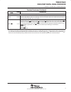
†
I = input, O = output, Z = high impedance, S = supply
‡
All revisions of the ’5402 can be operated with an external clock source, provided that the proper voltage levels be driven on the X2/CLKIN
pin. It should be noted that the X2/CLKIN pin is referenced to the device 1.8V power supply (CV
DD
), rather than the 3V I/O supply (DV
DD
).
Refer to the recommended operating conditions section of this document for the allowable voltage levels of the X2/CLKIN pin.