


TMS320VC5402
FIXEDĆPOINT DIGITAL SIGNAL PROCESSOR
SPRS079E – OCTOBER 1998 – REVISED AUGUST 2000
41
POST OFFICE BOX 1443 • HOUSTON, TEXAS 77251–1443
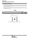
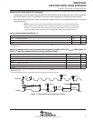
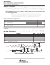
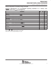
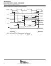
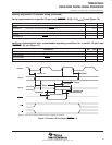
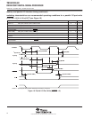
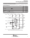
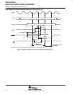
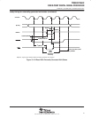
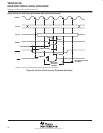
memory and parallel I/O interface timing (continued)
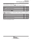
switching characteristics over recommended operating conditions for a
memory write
(MSTRB
= 0)
[H = 0.5 t
c(CO)
]
†
(see Figure 14)
PARAMETER MIN MAX UNIT
t
d(CLKH-A)
Delay time, CLKOUT high to address valid
‡
–2 3 ns
t
d(CLKL-A)
Delay time, CLKOUT low to address valid
§
–2 3 ns
t
d(CLKL-MSL)
Delay time, CLKOUT low to MSTRB low –1 3 ns
t
d(CLKL-D)W
Delay time, CLKOUT low to data valid 0 6 ns
t
d(CLKL-MSH)
Delay time, CLKOUT low to MSTRB high –1 3 ns
t
d(CLKH-RWL)
Delay time, CLKOUT high to R/W low –1 3 ns
t
d(CLKH-RWH)
Delay time, CLKOUT high to R/W high –1 3 ns
t
d(RWL-MSTRBL)
Delay time, R/W low to MSTRB low H – 2 H + 1 ns
t
h(A)W
Hold time, address valid after CLKOUT high
‡
1 3 ns
t
h(D)MSH
Hold time, write data valid after MSTRB high H–3 H+6
§
ns
t
w(SL)MS
Pulse duration, MSTRB low 2H–2 ns
t
su(A)W
Setup time, address valid before MSTRB low 2H–2 ns
t
su(D)MSH
Setup time, write data valid before MSTRB high 2H–6 2H+5
§
ns
t
en(D–RWL)
Enable time, data bus driven after R/W low H–5 ns
t
dis(RWH–D)
Disable time, R/W high to data bus high impedance 0 ns
†
Address, PS, and DS timings are all included in timings referenced as address.
‡
In the case of a memory write preceded by a memory write
§
In the case of a memory write preceded by an I/O cycle