


TMS320VC5402
FIXEDĆPOINT DIGITAL SIGNAL PROCESSOR
SPRS079E – OCTOBER 1998 – REVISED AUGUST 2000
38
POST OFFICE BOX 1443 • HOUSTON, TEXAS 77251–1443
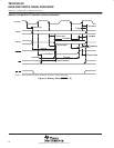
multiply-by-N clock option
The frequency of the reference clock provided at the X2/CLKIN pin can be multiplied by a factor of N to generate
the internal machine cycle. The selection of the clock mode and the value of N is described in the clock generator
section.
When an external clock source is used, the external frequency injected must conform to specifications listed
in the timing requirements table.
NOTE:All revisions of the ’5402 can be operated with an external clock source, provided that the proper
voltage levels be driven on the X2/CLKIN pin. It should be noted that the X2/CLKIN pin is referenced to
the device 1.8V power supply (CVdd), rather than the 3V I/O supply (DVdd). Refer to the recommended
operating conditions section of this document for the allowable voltage levels of the X2/CLKIN pin.
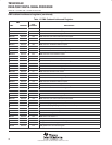
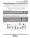
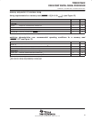
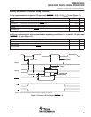
timing requirements (see Figure 12)
†
MIN MAX UNIT
Integer PLL multiplier N (N = 1–15) 20
‡
200
t
c
(
CI
)
Cycle time, X2/CLKIN
PLL multiplier N = x.5
20
‡
100
ns
t
c(CI)
Cycle
time
,
X2/CLKIN
PLL multiplier N = x.25, x.75 20
‡
50
ns
t
f(CI)
Fall time, X2/CLKIN 8 ns
t
r(CI)
Rise time, X2/CLKIN 8 ns
†
N = Multiplication factor
‡
The multiplication factor and minimum X2/CLKIN cycle time should be chosen such that the resulting CLKOUT cycle time is within the specified
range (tc(CO))
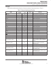
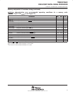
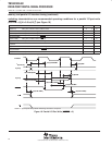
switching characteristics over recommended operating conditions [H = 0.5t
c(CO)
]
(see Figure 10 and Figure 12)
PARAMETER MIN TYP MAX UNIT
t
c(CO)
Cycle time, CLKOUT 10 t
c(CI)/N
†
ns
t
d(CI-CO)
Delay time, X2/CLKIN high/low to CLKOUT high/low 4 10 17 ns
t
f(CO)
Fall time, CLKOUT 2 ns
t
r(CO)
Rise time, CLKOUT 2 ns
t
w(COL)
Pulse duration, CLKOUT low H–2 H ns
t
w(COH)
Pulse duration, CLKOUT high H–2 H ns
t
p
Transitory phase, PLL lock up time 30 ms
†
N = Multiplication factor
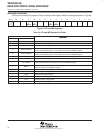
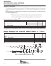
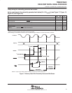
t
c(CO)
t
c(CI)
t
w(COH)
t
f(CO)
t
r(CO)
t
f(CI)
X2/CLKIN
CLKOUT
t
d(CI-CO)
t
w(COL)
t
r(CI)
tp
Unstable
Figure 12. External Multiply-by-One Clock Timing