


TMS320VC5402
FIXEDĆPOINT DIGITAL SIGNAL PROCESSOR
SPRS079E – OCTOBER 1998 – REVISED AUGUST 2000
54
POST OFFICE BOX 1443 • HOUSTON, TEXAS 77251–1443
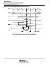
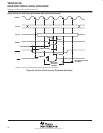
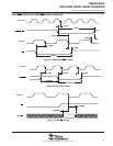
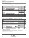
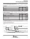
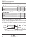
multichannel buffered serial port timing
timing requirements for McBSP [H=0.5t
c(CO)
]
†
(see Figure 28 and Figure 29)
MIN MAX UNIT
t
c(BCKRX)
Cycle time, BCLKR/X BCLKR/X ext 4H ns
t
w(BCKRX)
Pulse duration, BCLKR/X high or BCLKR/X low BCLKR/X ext 2H–2 ns
t
Setup time external BFSR high before BCLKR low
BCLKR int 8
ns
t
su(BFRH-BCKRL)
Setup time, external BFSR high before BCLKR low
BCLKR ext
1
ns
t
Hold time external BFSR high after BCLKR low
BCLKR int 0
ns
t
h(BCKRL-BFRH)
Hold time, external BFSR high after BCLKR low
BCLKR ext
3
ns
t
Setup time BDR valid before BCLKR low
BCLKR int 5
ns
t
su(BDRV-BCKRL)
Setup time, BDR valid before BCLKR low
BCLKR ext
0
ns
t
Hold time BDR valid after BCLKR low
BCLKR int 0
ns
t
h(BCKRL-BDRV)
Hold time, BDR valid after BCLKR low
BCLKR ext
4
ns
t
Setup time external BFSX high before BCLKX low
BCLKX int 7
ns
t
su(BFXH-BCKXL)
Setup time, external BFSX high before BCLKX low
BCLKX ext
0
ns
t
Hold time external BFSX high after BCLKX low
BCLKX int 0
ns
t
h(BCKXL-BFXH)
Hold time, external BFSX high after BCLKX low
BCLKX ext
3
ns
t
r(BCKRX)
Rise time, BCKR/X BCLKR/X ext 8 ns
t
f(BCKRX)
Fall time, BCKR/X BCLKR/X ext 8 ns
†
CLKRP = CLKXP = FSRP = FSXP = 0. If the polarity of any of the signals is inverted, then the timing references of that signal are also inverted.
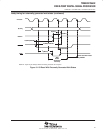
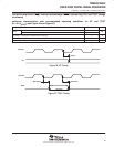
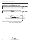
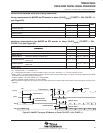
switching characteristics for McBSP [H=0.5t
c(CO)
]
†
(see Figure 28 and Figure 29)
PARAMETER MIN MAX UNIT
t
c(BCKRX)
Cycle time, BCLKR/X BCLKR/X int 4H ns
t
w(BCKRXH)
Pulse duration, BCLKR/X high BCLKR/X int D – 2
‡
D + 2
‡
ns
t
w(BCKRXL)
Pulse duration, BCLKR/X low BCLKR/X int C – 2
‡
C + 2
‡
ns
t
Delay time BCLKR high to internal BFSR valid
BCLKR int –2 2 ns
t
d(BCKRH-BFRV)
Delay time, BCLKR high to internal BFSR valid
BCLKR ext
3 9 ns
t
Delay time BCLKX high to internal BFSX valid
BCLKX int 0 4
ns
t
d(BCKXH-BFXV)
Delay time, BCLKX high to internal BFSX valid
BCLKX ext
8 11
ns
t
Disable time, BCLKX hi
g
h to BDX hi
g
h impedance followin
g
last data
BCLKX int –1 4
ns
t
dis(BCKXH-BDXHZ)
Disable
time
,
BCLKX
high
to
BDX
high
im edance
following
last
data
bit of transfer
BCLKX ext
3 9
ns
t
Delay time BCLKX high to BDX valid
DXENA 0
§
BCLKX int 0
¶
7
ns
t
d(BCKXH-BDXV)
Delay time, BCLKX high to BDX valid
DXENA = 0
§
BCLKX ext 3 11
ns
t
Delay time, BFSX high to BDX valid
BFSX int –1
¶
3
ns
t
d(BFXH-BDXV)
ONLY applies when in data delay 0 (XDATDLY = 00b) mode
BFSX ext 3 13
ns
†
CLKRP = CLKXP = FSRP = FSXP = 0. If the polarity of any of the signals is inverted, then the timing references of that signal are also inverted.
‡
T = BCLKRX period = (1 + CLKGDV) * 2H
C = BCLKRX low pulse width = T/2 when CLKGDV is odd or zero and = (CLKGDV/2) * 2H when CLKGDV is even
D = BCLKRX high pulse width = T/2 when CLKGDV is odd or zero and = (CLKGDV/2 + 1) * 2H when CLKGDV is even
§
The transmit delay enable (DXENA) and A–bis mode (ABIS) features of the McBSP are not implemented on the TMS320VC5402.
¶
Minimum delay times also represent minimum output hold times.