


TMS320VC5402
FIXEDĆPOINT DIGITAL SIGNAL PROCESSOR
SPRS079E – OCTOBER 1998 – REVISED AUGUST 2000
22
POST OFFICE BOX 1443 • HOUSTON, TEXAS 77251–1443
clock generator (continued)
The reference clock input is then divided by two (DIV mode) to generate clocks for the ’5402 device, or the PLL
circuit can be used (PLL mode) to generate the device clock by multiplying the reference clock frequency by
a scale factor, allowing use of a clock source with a lower frequency than that of the CPU.The PLL is an adaptive
circuit that, once synchronized, locks onto and tracks an input clock signal.
When the PLL is initially started, it enters a transitional mode during which the PLL acquires lock with the input
signal. Once the PLL is locked, it continues to track and maintain synchronization with the input signal. Then,
other internal clock circuitry allows the synthesis of new clock frequencies for use as master clock for the ’5402
device.
This clock generator allows system designers to select the clock source. The sources that drive the clock
generator are:
D A crystal resonator circuit. The crystal resonator circuit is connected across the X1 and X2/CLKIN pins of
the ’5402 to enable the internal oscillator.
D An external clock. The external clock source is directly connected to the X2/CLKIN pin, and X1 is left
unconnected.
NOTE: All revisions of the ’5402 can be operated with an external clock source, provided that the proper voltage
levels be driven on the X2/CLKIN pin. It should be noted that the X2/CLKIN pin is referenced to the device 1.8V
power supply (CVdd), rather than the 3V I/O supply (DVdd). Refer to the recommended operating conditions
section of this document for the allowable voltage levels of the X2/CLKIN pin.
The software-programmable PLL features a high level of flexibility, and includes a clock scaler that provides
various clock multiplier ratios, capability to directly enable and disable the PLL, and a PLL lock timer that can
be used to delay switching to PLL clocking mode of the device until lock is achieved.Devices that have a built-in
software-programmable PLL can be configured in one of two clock modes:
D PLL mode. The input clock (X2/CLKIN) is multiplied by 1 of 31 possible ratios. These ratios are achieved
using the PLL circuitry.
D DIV (divider) mode. The input clock is divided by 2 or 4. Note that when DIV mode is used, the PLL can be
completely disabled in order to minimize power dissipation.
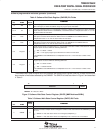
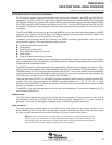
The software-programmable PLL is controlled using the 16-bit memory-mapped (address 0058h) clock mode
register (CLKMD). The CLKMD register is used to define the configuration of the PLL clock module. Upon reset,
the CLKMD register is initialized with a predetermined value dependent only upon the state of the CLKMD1 –
CLKMD3 pins as shown in Table 5.
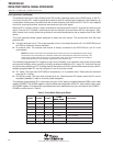
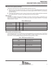
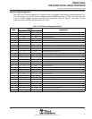
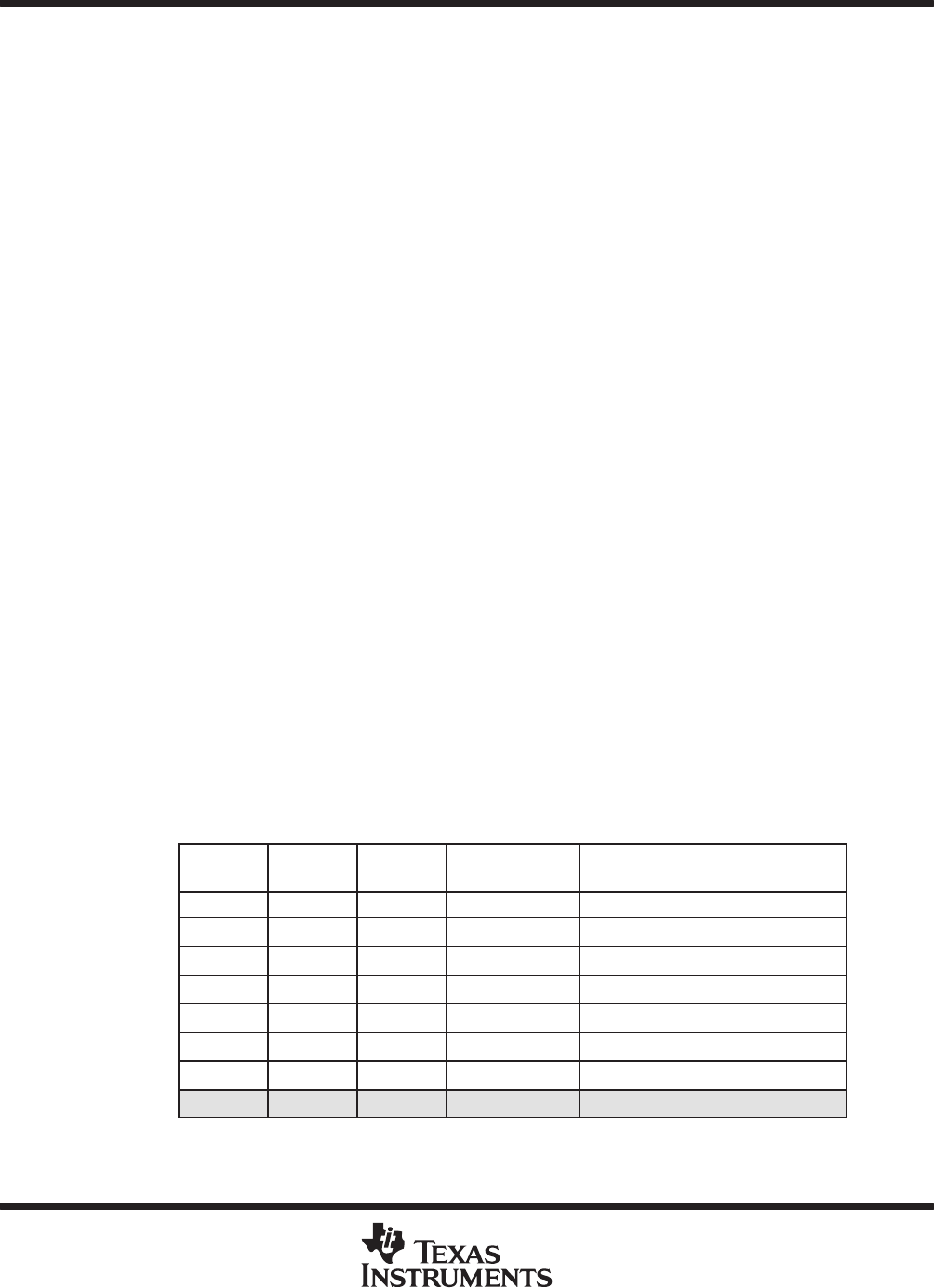
Table 5. Clock Mode Settings at Reset
CLKMD1 CLKMD2 CLKMD3
CLKMD
RESET VALUE
CLOCK MODE
CLKMD1
CLKMD2
CLKMD3
RESET VALUE
CLOCK
MODE
0 0 0 E007h PLL x 15
0 0 1 9007h PLL x 10
0 1 0 4007h PLL x 5
1 0 0 1007h PLL x 2
1 1 0 F007h PLL x 1
1 1 1 0000h 1/2 (PLL disabled)
1 0 1 F000h 1/4 (PLL disabled)
0 1 1 — Reserved (bypass mode)