


TMS320VC5402
FIXEDĆPOINT DIGITAL SIGNAL PROCESSOR
SPRS079E – OCTOBER 1998 – REVISED AUGUST 2000
8
POST OFFICE BOX 1443 • HOUSTON, TEXAS 77251–1443
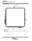
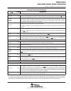
Terminal Functions (Continued)
TERMINAL
NAME
DESCRIPTIONTYPE
†
TERMINAL
NAME
DESCRIPTIONTYPE
†
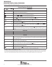
INITIALIZATION, INTERRUPT, AND RESET OPERATIONS (CONTINUED)
RS
I
Reset. RS causes the digital signal processor (DSP) to terminate execution and causes a reinitialization of the
CPU and peripherals. When RS
is brought to a high level, execution begins at location 0FF80h of program
memory. RS
affects various registers and status bits.
MP/MC I
Microprocessor/microcomputer mode select. If active low at reset, microcomputer mode is selected, and the
internal program ROM is mapped into the upper 4K words of program memory space. If the pin is driven high
during reset, microprocessor mode is selected, and the on-chip ROM is removed from program space. This pin
is only sampled at reset, and the MP/MC
bit of the processor mode status (PMST) register can override the mode
that is selected at reset.
MULTIPROCESSING SIGNALS
BIO I
Branch control. A branch can be conditionally executed when BIO is active. If low, the processor executes the
conditional instruction. For the XC instruction, the BIO
condition is sampled during the decode phase of the
pipeline; all other instructions sample BIO
during the read phase of the pipeline.
XF O/Z
External flag output (latched software-programmable signal). XF is set high by the SSBX XF instruction, set low
by the RSBX XF instruction or by loading ST1. XF is used for signaling other processors in multiprocessor
configurations or used as a general-purpose output pin. XF goes into the high-impedance state when OFF
is
low, and is set high at reset.
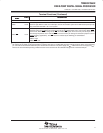
MEMORY CONTROL SIGNALS
DS
PS
IS
O/Z
Data, program, and I/O space select signals. DS, PS, and IS are always high unless driven low for accessing
a particular external memory space. Active period corresponds to valid address information. DS
, PS, and IS are
placed into the high-impedance state in the hold mode; the signals also go into the high-impedance state when
OFF
is low.
MSTRB O/Z
Memory strobe signal. MSTRB is always high unless low-level asserted to indicate an external bus access to
data or program memory. MSTRB
is placed in the high-impedance state in the hold mode; it also goes into the
high-impedance state when OFF
is low.
READY I
Data ready. READY indicates that an external device is prepared for a bus transaction to be completed. If the
device is not ready (READY is low), the processor waits one cycle and checks READY again. Note that the
processor performs ready detection if at least two software wait states are programmed. The READY signal is
not sampled until the completion of the software wait states.
R/W O/Z
Read/write signal. R/W indicates transfer direction during communication to an external device. R/W is normally
in the read mode (high), unless it is asserted low when the DSP performs a write operation. R/W
is placed in
the high-impedance state in hold mode; it also goes into the high-impedance state when OFF
is low.
IOSTRB O/Z
I/O strobe signal. IOSTRB is always high unless low-level asserted to indicate an external bus access to an I/O
device. IOSTRB
is placed in the high-impedance state in the hold mode; it also goes into the high-impedance
state when OFF
is low.
HOLD I
Hold. HOLD is asserted to request control of the address, data, and control lines. When acknowledged by the
’C54x, these lines go into the high-impedance state.
HOLDA O/Z
Hold acknowledge. HOLDA indicates that the ’5402 is in a hold state and that the address, data, and control lines
are in the high-impedance state, allowing the external memory interface to be accessed by other devices.
HOLDA
also goes into the high-impedance state when OFF is low.
MSC O/Z
Microstate complete. MSC indicates completion of all software wait states. When two or more software wait
states are enabled, the MSC
pin goes active at the beginning of the first software wait state and goes inactive
high at the beginning of the last software wait state. If connected to the READY input, MSC
forces one external
wait state after the last internal wait state is completed. MSC
also goes into the high-impedance state when OFF
is low.
IAQ O/Z
Instruction acquisition signal. IAQ is asserted (active low) when there is an instruction address on the address
bus. IAQ
goes into the high-impedance state when OFF is low.
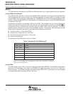
†
I = input, O = output, Z = high impedance, S = supply
‡
All revisions of the ’5402 can be operated with an external clock source, provided that the proper voltage levels be driven on the X2/CLKIN
pin. It should be noted that the X2/CLKIN pin is referenced to the device 1.8V power supply (CV
DD
), rather than the 3V I/O supply (DV
DD
).
Refer to the recommended operating conditions section of this document for the allowable voltage levels of the X2/CLKIN pin.