


TMS320VC5402
FIXEDĆPOINT DIGITAL SIGNAL PROCESSOR
SPRS079E – OCTOBER 1998 – REVISED AUGUST 2000
34
POST OFFICE BOX 1443 • HOUSTON, TEXAS 77251–1443
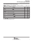
absolute maximum ratings over specified temperature range (unless otherwise noted)
†
Supply voltage I/O range, DV
DD
‡ –0.3 V to 4.0 V. . . . . . . . . . . . . . . . . . . . . . . . . . . . . . . . . . . . . . . . . . . . . . . . . . . .
Supply voltage core range, CV
DD
‡
–0.3 V to 2.4 V. . . . . . . . . . . . . . . . . . . . . . . . . . . . . . . . . . . . . . . . . . . . . . . . . .
Input voltage range, V
I
–0.3 V to 4.5 V. . . . . . . . . . . . . . . . . . . . . . . . . . . . . . . . . . . . . . . . . . . . . . . . . . . . . . . . . . . . .
Output voltage range, V
O
–0.3 V to 4.5 V. . . . . . . . . . . . . . . . . . . . . . . . . . . . . . . . . . . . . . . . . . . . . . . . . . . . . . . . . . .
Operating case temperature range, T
C
–40°C to 100°C. . . . . . . . . . . . . . . . . . . . . . . . . . . . . . . . . . . . . . . . . . . . . .
Storage temperature range, T
stg
–55°C to 150°C. . . . . . . . . . . . . . . . . . . . . . . . . . . . . . . . . . . . . . . . . . . . . . . . . . . .
†
Stresses beyond those listed under “absolute maximum ratings” may cause permanent damage to the device. These are stress ratings only, and
functional operation of the device at these or any other conditions beyond those indicated under “recommended operating conditions” is not
implied. Exposure to absolute-maximum-rated conditions for extended periods may affect device reliability.
‡
All voltage values are with respect to V
SS
.
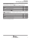
recommended operating conditions
MIN NOM MAX UNIT
DV
DD
Device supply voltage, I/O
§
3 3.3 3.6 V
CV
DD
Device supply voltage, core
§
1.71 1.8 1.98 V
V
SS
Supply voltage, GND 0 V
High level input voltage
RS, INTn, NMI, BIO, BCLKR0, BCLKR1,
BCLKX0, BCLKX1, HCS
, HDS1, HDS2, TDI,
TMS, CLKMDn
2.2 DV
DD
+ 0.3
V
IH
High-level input voltage
DV
DD
= 3.3"0.3 V
X2/CLKIN
¶
1.35 CV
DD
+0.3
V
DV
DD
=
3
.
3"0
.
3
V
TCK, TRST 2.5 DV
DD
+ 0.3
All other inputs 2 DV
DD
+ 0.3
V
IL
Low-level input voltage
DV
DD
= 3.3"0.3 V
RS, INTn, NMI, X2/CLKIN
¶
, BIO, BCLKR0,
BCLKR1, BCLKX0, BCLKX1, HCS
, HDS1,
HDS2
, TCK, CLKMDn
–0.3 0.6
V
DV
DD
=
3
.
3"0
.
3
V
All other inputs –0.3 0.8
I
OH
High-level output current –300 µA
I
OL
Low-level output current 1.5 mA
T
C
Operating case temperature –40 100 °C
§
Texas Instrument DSPs do not require specific power sequencing between the core supply and the I/O supply. However, systems should be
designed to ensure that neither supply is powered up for extended periods of time if the other supply is below the proper operating voltage.
Excessive exposure to these conditions can adversely affect the long term reliability of the devices. System-level concerns such as bus contention
may require supply sequencing to be implemented. In this case, the core supply should be powered up at the same time as or prior to the I/O
buffers and then powered down after the I/O buffers.
¶
All revisions of the ’5402 can be operated with an external clock source, provided that the proper voltage levels be driven on the X2/CLKIN pin.
It should be noted that the X2/CLKIN pin is referenced to the device 1.8V power supply (CVdd), rather than the 3V I/O supply (DVdd). Refer to
the recommended operating conditions section of this document for the allowable voltage levels of the X2/CLKIN pin.