


TMS320VC5402
FIXEDĆPOINT DIGITAL SIGNAL PROCESSOR
SPRS079E – OCTOBER 1998 – REVISED AUGUST 2000
21
POST OFFICE BOX 1443 • HOUSTON, TEXAS 77251–1443
multichannel buffered serial ports (continued)
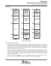
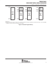
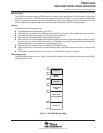
On the receiver, receive frame synchronization and clocking are indicated by the BFSR and BCLKR pins,
respectively. The CPU or DMA can read received data from the data receive register (DRR). Data received on
the BDR pin is shifted into a receive shift register (RSR) and then buffered in the receive buffer register (RBR).
If the DRR is empty, the RBR contents are copied into the DRR. If not, the RBR holds the data until the DRR
is available. This structure allows storage of the two previous words while the reception of the current word is
in progress.
The CPU and DMA can move data to and from the McBSPs and can synchronize transfers based on McBSP
interrupts, event signals, and status flags. The DMA is capable of handling data movement between the
McBSPs and memory with no intervention from the CPU.
In addition to the standard serial port functions, the McBSP provides programmable clock and frame
synchronization signals. The programmable functions include:
D Frame synchronization pulse width
D Frame period
D Frame synchronization delay
D Clock reference (internal vs. external)
D Clock division
D Clock and frame synchronization polarity
The on-chip companding hardware allows compression and expansion of data in either µ-law or A-law format.
When companding is used, transmit data is encoded according to specified companding law and received data
is decoded to 2s complement format.
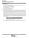
The McBSP allows the multiple channels to be independently selected for the transmitter and receiver. When
multiple channels are selected, each frame represents a time-division multiplexed (TDM) data stream. In using
TDM data streams, the CPU may only need to process a few of them. Thus, to save memory and bus bandwidth,
multichannel selection allows independent enabling of particular channels for transmission and reception. Up
to 32 channels in a stream of up to 128 channels can be enabled.
The clock-stop mode (CLKSTP) in the McBSP provides compatibility with the serial peripheral interface (SPI)
protocol. The word sizes supported by the McBSP are programmable for 8-, 12-, 16-, 20-, 24-, or 32-bit
operation. When the McBSP is configured to operate in SPI mode, both the transmitter and the receiver operate
together as a master or as a slave.
The McBSP is fully static and operates at arbitrarily low clock frequencies. The maximum frequency is CPU
clock frequency divided by 2.
hardware timer
The ’5402 device features two 16-bit timing circuits with 4-bit prescalers. The main counter of each timer is
decremented by one every CLKOUT cycle. Each time the counter decrements to 0, a timer interrupt is
generated. The timers can be stopped, restarted, reset, or disabled by specific control bits.
clock generator
The clock generator provides clocks to the ’5402 device, and consists of an internal oscillator and a
phase-locked loop (PLL) circuit. The clock generator requires a reference clock input, which can be provided
by using a crystal resonator with the internal oscillator, or from an external clock source.
NOTE:All revisions of the ’5402 can be operated with an external clock source, provided that the proper voltage
levels be driven on the X2/CLKIN pin. It should be noted that the X2/CLKIN pin is referenced to the device 1.8V
power supply (CVdd), rather than the 3V I/O supply (DVdd). Refer to the recommended operating conditions
section of this document for the allowable voltage levels of the X2/CLKIN pin.