


TMS320VC5402
FIXEDĆPOINT DIGITAL SIGNAL PROCESSOR
SPRS079E – OCTOBER 1998 – REVISED AUGUST 2000
18
POST OFFICE BOX 1443 • HOUSTON, TEXAS 77251–1443
programmable bank-switching wait states
The programmable bank-switching logic of the ’5402 is functionally equivalent to that of the ’548/’549 devices.
This feature automatically inserts one cycle when accesses cross memory-bank boundaries within program or
data memory space. A bank-switching wait state can also be automatically inserted when accesses cross the
data space boundary into program space.
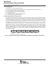
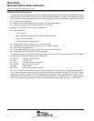
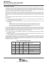
The bank-switching control register (BSCR) defines the bank size for bank-switching wait states. Figure 6
shows the BSCR and its bits are described in Table 4.
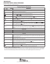
BNKCMP PS-DS Reserved HBH
12 11 3 2 115
R/W-0R-0R/W-1R/W-1111
BH
EXIO
010
R/W-0R/W-0
LEGEND: R = Read, W = Write
Figure 6. Bank-Switching Control Register (BSCR), MMR Address 0029h
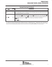
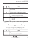
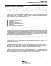
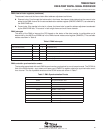
Table 4. Bank-Switching Control Register (BSCR) Fields
BIT
RESET
FUNCTION
NO. NAME
RESET
VALUE
FUNCTION
15–12 BNKCMP 1111
Bank compare. Determines the external memory-bank size. BNKCMP is used to mask the four MSBs of
an address. For example, if BNKCMP = 1111b, the four MSBs (bits 12–15) are compared, resulting in a
bank size of 4K words. Bank sizes of 4K words to 64K words are allowed.
11 PS - DS 1
Program read – data read access. Inserts an extra cycle between consecutive accesses of program read
and data read or data read and program read.
PS-DS = 0 No extra cycles are inserted by this feature.
PS-DS = 1 One extra cycle is inserted between consecutive data and program reads.
10–3 Reserved 0 These bits are reserved and are unaffected by writes.
2 HBH 0
HPI Bus holder. Controls the HPI bus holder feature. HBH is cleared to 0 at reset.
HBH = 0 The bus holder is disabled.
HBH = 1 The bus holder is enabled. When not driven, the HPI data bus (HD[7:0]) is held in the
previous logic level.
1 BH 0
Bus holder. Controls the data bus holder feature. BH is cleared to 0 at reset.
BH = 0 The bus holder is disabled.
BH = 1 The bus holder is enabled. When not driven, the data bus (D[15:0]) is held in the
previous logic level.
External bus interface off. The EXIO bit controls the external bus-off function.
EXIO = 0 The external bus interface functions as usual
0 EXIO 0
EXIO = 0 The external bus interface functions as usual.
EXIO = 1 The address bus, data bus, and control signals become inactive after completing the
c rrent b s c cle Note that the DROM MP/MC and OVLY bits in the PMST and the HM
current bus cycle. Note that the DROM, MP/MC, and OVLY bits in the PMST and the HM
bit of ST1 cannot be modified when the interface is disabled.