


TMS320VC5402
FIXEDĆPOINT DIGITAL SIGNAL PROCESSOR
SPRS079E – OCTOBER 1998 – REVISED AUGUST 2000
62
POST OFFICE BOX 1443 • HOUSTON, TEXAS 77251–1443
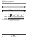
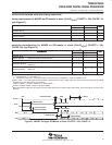
HPI8 timing (continued)
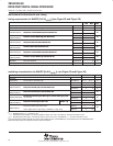
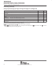
timing requirements
†‡§
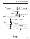
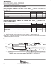
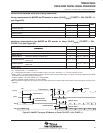
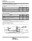
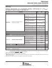
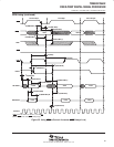
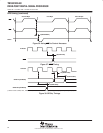
(see Figure 35, Figure 36, Figure 37, and Figure 38)
MIN MAX UNIT
t
su(HBV-DSL)
Setup time, HBIL and HAD valid before DS low or before HAS low
¶#
5 ns
t
h(DSL-HBV)
Hold time, HBIL and HAD valid after DS low or after HAS low
¶#
5 ns
t
su(HSL-DSL)
Setup time, HAS low before DS low 10 ns
t
w(DSL)
Pulse duration, DS low 20 ns
t
w(DSH)
Pulse duration, DS high 10 ns
t
su(HDV-DSH)
Setup time, HDx valid before DS high, HPI write 2 ns
t
h(DSH-HDV)W
Hold time, HDx valid after DS high, HPI write 3 ns
t
su(GPIO-COH)
Setup time, HDx input valid before CLKOUT high, HDx configured as general-purpose input 6 ns
t
h(GPIO-COH)
Hold time, HDx input valid after CLKOUT high, HDx configured as general-purpose input 0 ns
†
DS refers to the logical OR of HCS, HDS1, and HDS2.
‡
HDx refers to any of the HPI data bus pins (HD0, HD1, HD2, etc.).
§
GPIO refers to the HD pins when they are configured as general-purpose input/outputs.
¶
HAD
refers to HCNTL0, HCNTL1, and H/RW.
#
When the HAS
signal is used to latch the control signals, this timing refers to the falling edge of the HAS signal. Otherwise, when HAS is not used
(always high), this timing refers to the falling edge of DS.