


TMS320VC5402
FIXEDĆPOINT DIGITAL SIGNAL PROCESSOR
SPRS079E – OCTOBER 1998 – REVISED AUGUST 2000
7
POST OFFICE BOX 1443 • HOUSTON, TEXAS 77251–1443
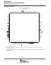
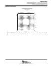
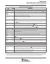
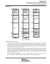
terminal functions
The following table lists each signal, function, and operating mode(s) grouped by function.
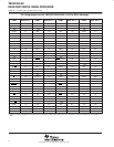
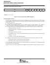
Terminal Functions
TERMINAL
TYPE
†
DESCRIPTION
TERMINAL
NAME
TYPE
†
DESCRIPTION
DATA SIGNALS
A19 (MSB)
A18
A17
A16
A15
A14
A13
A12
A11
A10
A9
A8
A7
A6
A5
A4
A3
A2
A1
A0 (LSB)
O/Z Parallel address bus A19 [most significant bit (MSB)] through A0 [least significant bit (LSB)]. The lower sixteen
address pins (A0 to A15) are multiplexed to address all external memory (program, data) or I/O, while the upper
four address pins (A16 to A19) are only used to address external program space. These pins are placed in the
high-impedance state when the hold mode is enabled, or when OFF
is low.
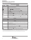
D15 (MSB)
D14
D13
D12
D11
D10
D9
D8
D7
D6
D5
D4
D3
D2
D1
D0 (LSB)
I/O/Z Parallel data bus D15 (MSB) through D0 (LSB). The sixteen data pins (D0 to D15) are multiplexed to transfer
data between the core CPU and external data/program memory or I/O devices. The data bus is placed in the
high-impedance state when not outputting or when RS
or HOLD is asserted. The data bus also goes into the
high-impedance state when OFF
is low.
The data bus has bus holders to reduce the static power dissipation caused by floating, unused pins. These bus
holders also eliminate the need for external bias resistors on unused pins. When the data bus is not being driven
by the ’5402, the bus holders keep the pins at the previous logic level. The data bus holders on the ’5402 are
disabled at reset and can be enabled/disabled via the BH bit of the bank-switching control register (BSCR).
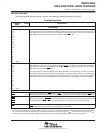
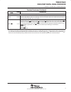
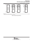
INITIALIZATION, INTERRUPT, AND RESET OPERATIONS
IACK
O/Z
Interrupt acknowledge signal. IACK Indicates receipt of an interrupt and that the program counter is fetching the
interrupt vector location designated by A15–A0. IACK
also goes into the high-impedance state when OFF is low.
INT0
INT1
INT2
INT3
I
External user interrupts. INT0–INT3 are prioritized and are maskable by the interrupt mask register (IMR) and
the interrupt mode bit. INT0
–INT3 can be polled and reset by way of the interrupt flag register (IFR).
NMI
I
Nonmaskable interrupt. NMI is an external interrupt that cannot be masked by way of the INTM or the IMR. When
NMI
is activated, the processor traps to the appropriate vector location.
†
I = input, O = output, Z = high impedance, S = supply
‡
All revisions of the ’5402 can be operated with an external clock source, provided that the proper voltage levels be driven on the X2/CLKIN
pin. It should be noted that the X2/CLKIN pin is referenced to the device 1.8V power supply (CV
DD
), rather than the 3V I/O supply (DV
DD
).
Refer to the recommended operating conditions section of this document for the allowable voltage levels of the X2/CLKIN pin.