


TMS320VC5402
FIXEDĆPOINT DIGITAL SIGNAL PROCESSOR
SPRS079E – OCTOBER 1998 – REVISED AUGUST 2000
37
POST OFFICE BOX 1443 • HOUSTON, TEXAS 77251–1443
divide-by-two clock option (PLL disabled)
The frequency of the reference clock provided at the X2/CLKIN pin can be divided by a factor of two to generate
the internal machine cycle. The selection of the clock mode is described in the clock generator section.
When an external clock source is used, the frequency injected must conform to specifications listed in the timing
requirements table.
NOTE:All revisions of the ’5402 can be operated with an external clock source, provided that the proper
voltage levels be driven on the X2/CLKIN pin. It should be noted that the X2/CLKIN pin is referenced to
the device 1.8V power supply (CVdd), rather than the 3V I/O supply (DVdd). Refer to the recommended
operating conditions section of this document for the allowable voltage levels of the X2/CLKIN pin.
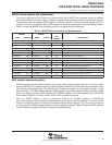
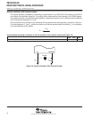
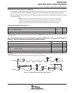
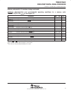
timing requirements (see Figure 11)
MIN MAX UNIT
t
c(CI)
Cycle time, X2/CLKIN 20
†
ns
t
f(CI)
Fall time, X2/CLKIN 8 ns
t
r(CI)
Rise time, X2/CLKIN 8 ns
†
This device utilizes a fully static design and therefore can operate with t
c(CI)
approaching ∞. The device is characterized at frequencies
approaching 0 Hz.
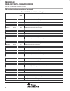
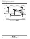
switching characteristics over recommended operating conditions [H = 0.5t
c(CO)
]
†
(see Figure 10,
Figure 11, and the recommended operating conditions table)
PARAMETER MIN TYP MAX UNIT
t
c(CO)
Cycle time, CLKOUT 10
‡
2t
c(CI)
†
ns
t
d(CIH-CO)
Delay time, X2/CLKIN high to CLKOUT high/low 4 10 17 ns
t
f(CO)
Fall time, CLKOUT 2 ns
t
r(CO)
Rise time, CLKOUT 2 ns
t
w(COL)
Pulse duration, CLKOUT low H–2 H ns
t
w(COH)
Pulse duration, CLKOUT high H–2 H ns
†
This device utilizes a fully static design and therefore can operate with t
c(CI)
approaching ∞. The device is characterized at frequencies
approaching 0 Hz.
‡
It is recommended that the PLL clocking option be used for maximum frequency operation.
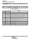
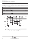
t
r(CO)
t
f(CO)
CLKOUT
X2/CLKIN
t
w(COL)
t
d(CIH-CO)
t
f(CI)
t
r(CI)
t
c(CO)
t
c(CI)
t
w(COH)
Figure 11. External Divide-by-Two Clock Timing