


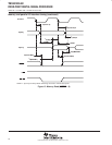
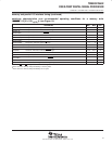

TMS320VC5402
FIXEDĆPOINT DIGITAL SIGNAL PROCESSOR
SPRS079E – OCTOBER 1998 – REVISED AUGUST 2000
35
POST OFFICE BOX 1443 • HOUSTON, TEXAS 77251–1443
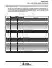
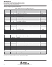
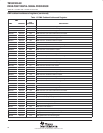
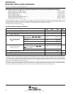
electrical characteristics over recommended operating case temperature range (unless otherwise
noted)
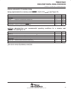
PARAMETER TEST CONDITIONS MIN TYP
†
MAX UNIT
V
OH
High-level output voltage
I
OH
= MAX 2.4 V
V
OL
Low-level output voltage I
OL
= MAX 0.4 V
I
IZ
Input current for
outputs in high
D[15:0], HD[7:0]
Bus holders enabled, DV
DD
= MAX,
V
I
= V
SS
to DV
DD
–175 175
µA
I
IZ
out uts
in
high
impedance
All other inputs
DV
DD
= MAX, V
O
= V
SS
to DV
DD
–5 5
µA
X2/CLKIN
}
–40 40
TRST With internal pulldown –5 300
I
I
Input current
HPIENA
With internal pulldown
(V
I
= V
SS
–5 300
µA
I
I
ucue
TMS, TCK, TDI, HPI
w
With internal pullups,
HPIENA = 0
(
ISS
to DV
DD
)
–300 5
µ
A
All other input only pins
5
5
All other input-only pins –5 5
I
DDC
Supply current, core CPU CV
DD
= 1.8 V, f
clock
= 100 MHz
¶
, T
C
= 25°C
#
45 mA
I
DDP
Supply current, pins DV
DD
= 3.3 V, f
clock
= 100 MHz
¶
, T
C
= 25°C
||
30 mA
I
DD
Supply current,
IDLE2 PLL × 1 mode, 100 MHz input 2 mA
I
DD
Su ly
current
,
standby
IDLE3
Divide-by-two mode, CLKIN stopped 20 µA
C
i
Input capacitance 5 pF
C
o
Output capacitance 5 pF
†
All values are typical unless otherwise specified.
‡
All revisions of the ’5402 can be operated with an external clock source, provided that the proper voltage levels be driven on the X2/CLKIN pin.
It should be noted that the X2/CLKIN pin is referenced to the device 1.8V power supply (CVdd), rather than the 3V I/O supply (DVdd). Refer to
the recommended operating conditions section of this document for the allowable voltage levels of the X2/CLKIN pin.
§
HPI input signals except for HPIENA.
¶
Clock mode: PLL × 1 with external source
#
This value represents the current consumption of the CPU, on-chip memory, and on-chip peripherals. Conditions include: program execution
from on-chip RAM, with 50% usage of MAC and 50% usage of NOP instructions. Actual operating current varies with program being executed.
||
This value was obtained using the following conditions: external memory writes at a rate of 20 million writes per second, CLKOFF=0, full-duplex
operation of McBSP0 and McBSP1 at a rate of 10 million bits per second each, and 15-pF loads on all outputs. For more details on how this
calculation is performed, refer to the
Calculation of TMS320C54x Power Dissipation Application Report
(literature number SPRA164).
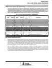
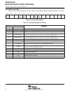
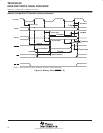
PARAMETER MEASUREMENT INFORMATION
Tester Pin
Electronics
V
Load
I
OL
C
T
I
OH
Output
Under
Test
50 Ω
Where: I
OL
= 1.5 mA (all outputs)
I
OH
= 300 µA (all outputs)
V
Load
= 1.5 V
C
T
= 40 pF typical load circuit capacitance
Figure 9. 3.3-V Test Load Circuit