


TMS320VC5402
FIXEDĆPOINT DIGITAL SIGNAL PROCESSOR
SPRS079E – OCTOBER 1998 – REVISED AUGUST 2000
12
POST OFFICE BOX 1443 • HOUSTON, TEXAS 77251–1443
memory
The ’5402 device provides both on-chip ROM and RAM memories to aid in system performance and integration.
on-chip ROM with bootloader
The ’5402 features a 4K-word × 16-bit on-chip maskable ROM. Customers can arrange to have the ROM of the
’5402 programmed with contents unique to any particular application. A security option is available to protect
a custom ROM. This security option is described in the
TMS320C54x DSP CPU and Peripherals Reference Set,
Volume 1
(literature number SPRU131). Note that only the ROM security option, and not the ROM/RAM option,
is available on the ’5402 .
A bootloader is available in the standard ’5402 on-chip ROM. This bootloader can be used to automatically
transfer user code from an external source to anywhere in the program memory at power up. If the MP/MC pin
is sampled low during a hardware reset, execution begins at location FF80h of the on-chip ROM. This location
contains a branch instruction to the start of the bootloader program. The standard ’5402 bootloader provides
different ways to download the code to accomodate various system requirements:
D Parallel from 8-bit or 16-bit-wide EPROM
D Parallel from I/O space 8-bit or 16-bit mode
D Serial boot from serial ports 8-bit or 16-bit mode
D Host-port interface boot
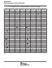
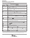
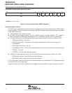
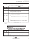
The standard on-chip ROM layout is shown in Table 1.
Table 1. Standard On-Chip ROM Layout
†
ADDRESS RANGE DESCRIPTION
F000h – F7FFh Reserved
F800h – FBFFh Bootloader
FC00h – FCFFh µ-law expansion table
FD00h – FDFFh A-law expansion table
FE00h – FEFFh Sine look-up table
FF00h – FF7Fh Reserved
FF80h – FFFFh Interrupt vector table
†
In the ’VC5402 ROM, 128 words are reserved for factory device-testing purposes. Application
code to be implemented in on-chip ROM must reserve these 128 words at addresses
FF00h–FF7Fh in program space.
on-chip RAM
The ’5402 device contains 16K
× 16-bit of on-chip dual-access RAM (DARAM). The DARAM is composed of
two blocks of 8K words each. Each block in the DARAM can support two reads in one cycle, or a read and a
write in one cycle. The DARAM is located in the address range 0060h–3FFFh in data space, and can be mapped
into program/data space by setting the OVLY bit to one.