


TMS320VC5402
FIXEDĆPOINT DIGITAL SIGNAL PROCESSOR
SPRS079E – OCTOBER 1998 – REVISED AUGUST 2000
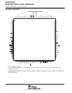
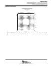
11
POST OFFICE BOX 1443 • HOUSTON, TEXAS 77251–1443
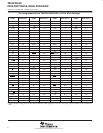
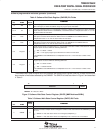
Terminal Functions (Continued)
TERMINAL
NAME
DESCRIPTIONTYPE
†
TERMINAL
NAME
DESCRIPTIONTYPE
†
TEST PINS (CONTINUED)
EMU0 I/O/Z
Emulator 0 pin. When TRST is driven low, EMU0 must be high for activation of the OFF condition. When TRST
is driven high, EMU0 is used as an interrupt to or from the emulator system and is defined as input/output by
way of the IEEE standard 1149.1 scan system.
EMU1/OFF I/O/Z
Emulator 1 pin/disable all outputs. When TRST is driven high, EMU1/OFF is used as an interrupt to or from the
emulator system and is defined as input/output by way of the IEEE standard 1149.1 scan system. When TRST
is driven low, EMU1/OFF is configured as OFF. The EMU1/OFF signal, when active low, puts all output drivers
into the high-impedance state. Note that OFF
is used exclusively for testing and emulation purposes (not for
multiprocessing applications). The OFF
feature is selected by the following pin combinations:
TRST
= low
EMU0 = high
EMU1/OFF
= low
†
I = input, O = output, Z = high impedance, S = supply
‡
All revisions of the ’5402 can be operated with an external clock source, provided that the proper voltage levels be driven on the X2/CLKIN
pin. It should be noted that the X2/CLKIN pin is referenced to the device 1.8V power supply (CV
DD
), rather than the 3V I/O supply (DV
DD
).
Refer to the recommended operating conditions section of this document for the allowable voltage levels of the X2/CLKIN pin.