


TMS320VC5402
FIXEDĆPOINT DIGITAL SIGNAL PROCESSOR
SPRS079E – OCTOBER 1998 – REVISED AUGUST 2000
10
POST OFFICE BOX 1443 • HOUSTON, TEXAS 77251–1443
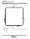
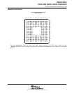
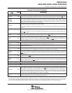
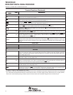
Terminal Functions (Continued)
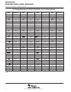
TERMINAL
NAME
DESCRIPTIONTYPE
†
TERMINAL
NAME
DESCRIPTIONTYPE
†
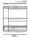
HOST-PORT INTERFACE SIGNALS (CONTINUED)
HBIL I
Byte identification. HBIL identifies the first or second byte of transfer. The HBIL input has an internal pullup
resistor that is only enabled when HPIENA = 0.
HCS I
Chip select. HCS is the select input for the HPI and must be driven low during accesses. The chip-select input
has an internal pullup resistor that is only enabled when HPIENA = 0.
HDS1
HDS2
I
Data strobe. HDS1 and HDS2 are driven by the host read and write strobes to control transfers. The strobe inputs
have internal pullup resistors that are only enabled when HPIENA = 0.
HAS I
Address strobe. Hosts with multiplexed address and data pins require HAS to latch the address in the HPIA
register. HAS
has an internal pullup resistor that is only enabled when HPIENA = 0.
HR/W I
Read/write. HR/W controls the direction of an HPI transfer. R/W has an internal pullup resistor that is only
enabled when HPIENA = 0.
HRDY O/Z
Ready. The ready output informs the host when the HPI is ready for the next transfer. HRDY goes into the
high-impedance state when OFF
is low.
HINT O/Z
Host interrupt. This output is used to interrupt the host. When the DSP is in reset, HINT is driven high. HINT can
also be configured as the timer 1 output (TOUT1), when the HPI is disabled. The signal goes into the
high-impedance state when OFF
is low.
HPIENA I
HPI module select. HPIENA must be driven high during reset to enable the HPI. An internal pulldown resistor
is always active and the HPIENA pin is sampled on the rising edge of RS
. If HPIENA is left open or is driven low
during reset, the HPI module is disabled. Once the HPI is disabled, the HPIENA pin has no effect until the ’5402
is reset.
SUPPLY PNS
CV
DD
S +V
DD
. Dedicated 1.8-V power supply for the core CPU
DV
DD
S +V
DD
. Dedicated 3.3-V power supply for the I/O pins
V
SS
S Ground
TEST PINS
TCK I
IEEE standard 1149.1 test clock. TCK is normally a free-running clock signal with a 50% duty cycle. The changes
on the test access port (TAP) of input signals TMS and TDI are clocked into the TAP controller, instruction
register, or selected test data register on the rising edge of TCK. Changes at the TAP output signal (TDO) occur
on the falling edge of TCK.
TDI I
IEEE standard 1149.1 test data input pin with internal pullup device. TDI is clocked into the selected register
(instruction or data) on a rising edge of TCK.
TDO O/Z
IEEE standard 1149.1 test data output. The contents of the selected register (instruction or data) are shifted out
of TDO on the falling edge of TCK. TDO is in the high-impedance state except when the scanning of data is in
progress. TDO also goes into the high-impedance state when OFF
is low.
TMS I
IEEE standard 1149.1 test mode select. Pin with internal pullup device. This serial control input is clocked into
the TAP controller on the rising edge of TCK.
TRST I
IEEE standard 1149.1 test reset. TRST, when high, gives the IEEE standard 1149.1 scan system control of the
operations of the device. If TRST
is not connected or is driven low, the device operates in its functional mode,
and the IEEE standard 1149.1 signals are ignored. Pin with internal pulldown device.
†
I = input, O = output, Z = high impedance, S = supply
‡
All revisions of the ’5402 can be operated with an external clock source, provided that the proper voltage levels be driven on the X2/CLKIN
pin. It should be noted that the X2/CLKIN pin is referenced to the device 1.8V power supply (CV
DD
), rather than the 3V I/O supply (DV
DD
).
Refer to the recommended operating conditions section of this document for the allowable voltage levels of the X2/CLKIN pin.