


TMS320VC5402
FIXEDĆPOINT DIGITAL SIGNAL PROCESSOR
SPRS079E – OCTOBER 1998 – REVISED AUGUST 2000
16
POST OFFICE BOX 1443 • HOUSTON, TEXAS 77251–1443
on-chip peripherals
The ’5402 device has the following peripherals:
D Software-programmable wait-state generator with programmable bank-switching wait states
D An enhanced 8-bit host-port interface (HPI8)
D Two multichannel buffered serial ports (McBSPs)
D Two hardware timers
D A clock generator with a phase-locked loop (PLL)
D A direct memory access (DMA) controller
software-programmable wait-state generator
The software wait-state generator of the ’5402 can extend external bus cycles by up to fourteen machine cycles.
Devices that require more than fourteen wait states can be interfaced using the hardware READY line. When
all external accesses are configured for zero wait states, the internal clocks to the wait-state generator are
automatically disabled. Disabling the wait-state generator clocks reduces the power comsumption of the ’5402.
The software wait-state register (SWWSR) controls the operation of the wait-state generator. The 14 LSBs of
the SWWSR specify the number of wait states (0 to 7) to be inserted for external memory accesses to five
separate address ranges. This allows a different number of wait states for each of the five address ranges.
Additionally, the software wait-state multiplier (SWSM) bit of the software wait-state control register (SWCR)
defines a multiplication factor of 1 or 2 for the number of wait states. At reset, the wait-state generator is initialized
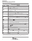
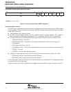
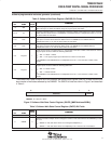
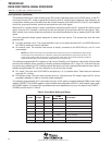
to provide seven wait states on all external memory accesses. The SWWSR bit fields are shown in Figure 4
and described in Table 2.
XPA I/O Data Data Program Program
14 12 11 9 8 6 5 3 2 015
R/W-111R/W-0 R/W-111 R/W-111 R/W-111 R/W-111
LEGEND: R=Read, W=Write, 0=Value after reset
Figure 4. Software Wait-State Register (SWWSR) [Memory-Mapped Register (MMR) Address 0028h]