


Copernicus GPS Receiver 71
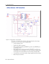
RF LAYOUT CONSIDERATIONS 6
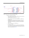
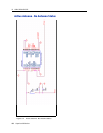
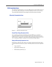
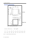
In the printed circuit board (PCB) layout, it is recommended to keep the copper layer
on which the Copernicus GPS Receiver is mounted clear of solder mask and copper
(vias or traces) under the module. This is to insure mating of the castellations between
the Copernicus GPS module and the board to which it is mounted, and that there is no
interference with features beneath the Copernicus GPS Receiver causing it to lift
during the re-flow solder process.
For a microstrip RF transmission line topology, it is recommended that the layer
immediately below the one to which the Copernicus GPS Receiver is mounted be
ground plane. Pins 2 and 4 should be directly connected to this ground plane with low
inductance connections. Pin 3, the RF input, can be routed on the top layer using the
proper geometry for a 50 ohm system.