


Copernicus GPS Receiver 103
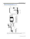
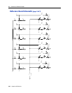
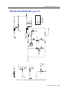
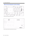
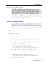
COPERNICUS REFERENCE BOARD 10
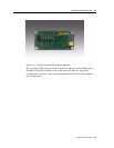
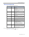
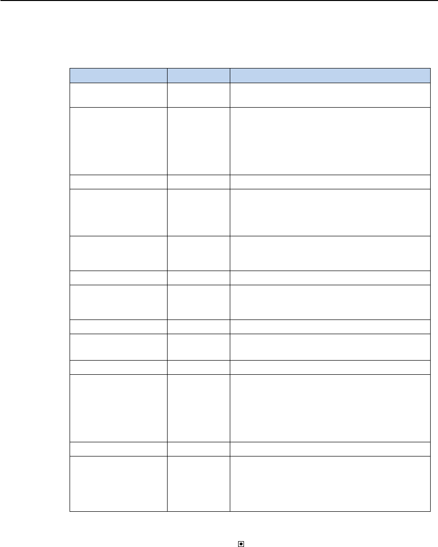
Reference Board Jumper Table
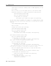
Table 10.2 Copernicus Reference Board Jumper Table
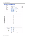
* See Copernicus Reference Board Schematics in this chapter.
Note – See Table 3.1 for pin numbers. indicates pin 1.
Reference Designator Name Description
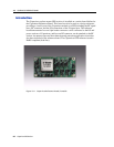
J1 RF Input MCX Jack (Female Connector)50 Ohms
unbalanced
J4 XRESET Normal Operation: Jumper in place (connects
XRESET to VCC)
Reset Operation: Removing the Jumper and
asserting pin 2 of J4 low for greater than 100 usec
resets the unit. *Switch SW1 can also reset the
unit. Please see below.
SW1 Reset Switch Press the button resets the unit.
J5 VCC Normal Operation: Jumper in place (Applies
VCC to unit)
Test Mode: Jumper may be removed and ampere
meter may be inserted for current measurement.
J6 Vback Normal Operation: Jumper in place.(Applies
VBack to unit). The user can use VCC as the
STANDBY Supply.
J7 8-Pin Header See Table 10 for Reference Board pin Description.
J8 PPS Normal Operation: Jumper in place.(It outputs
PPS at pin 9 of both DB9 connectors of the Starter
Kit through J7 pin 6 of the Reference Board).
J9-J21 Reserved Reserved
J25 Reserved Reserved
Normal Operation: No Jumper (Run Mode).
J27 Reserved Reserved
J28 XSTANDBY Normal Operation: Jumper between pins 1 and
2 of the jumper J28 (Run Mode). *
Standby Mode: Jumper between pins 2 and 3 of
J28. *For external control, Jumper may be
removed and pin 2 of the jumper can be
externally controlled, e.g. via a host processor.
J22-24 Spare Spare driver transistor
J26 Antenna
Power
Normal Operation: Jumper in place.(Active
antenna powered from VCC).If a separate power
supply is desired for active antenna, jumper may
be removed and an external antenna power can
be applied to pin 2 of J26. *