


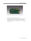

Copernicus GPS Receiver 99
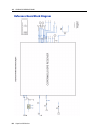
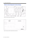
COPERNICUS REFERENCE BOARD 10
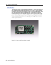
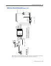
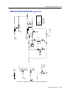
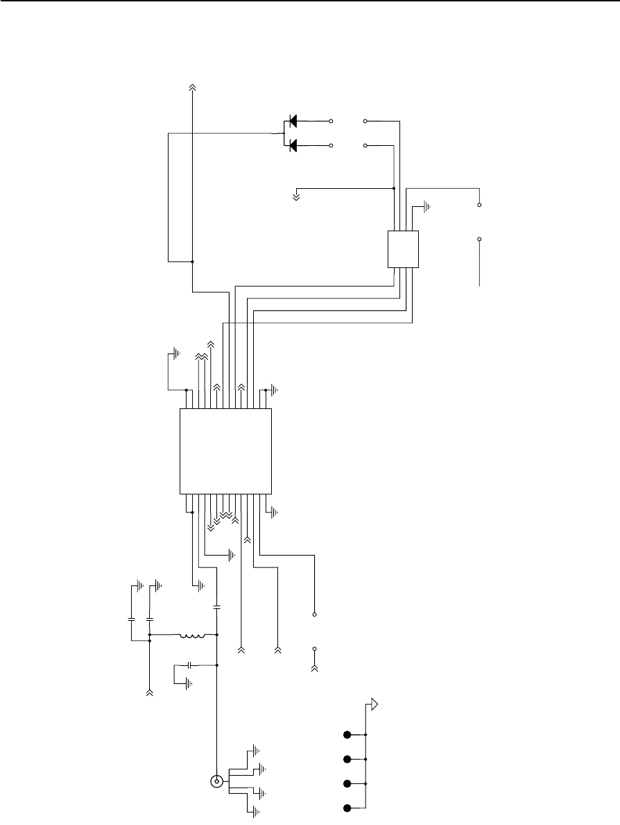
Reference Board Schematic (page 1 of 3)
Note – Reference board schematics may differ from the recommendations outlined in
Table 3.1 due to the test mode requirements for Trimble’s internal use.
PPS
PPS
BOOT
Vmain
XRESET
MONITOR
Vant
VLED
GPIO_A5
LNA_XEN
XSTANDBY
GPIO_A6
SHRT
GPIO_A11
OPN
GPIO_B5
GPIO_A10
GPIO_A4
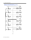
Minimum length 50 ohm trace
1: TXDB 2: 3.3V
3: TXDA 4: Vback
5: RXDA 6: PPS
7: RXDB 8: GND
NOTE: 24 jumpers are
required to be included
on the BOM and in the
Assembly Drawing.
*C1 and C4 are impedance matching components,
values depend on the PBC layout.
Copernicus RF_IN is internally DC-decoupled.
C4*
18pF
U1
Copernicus
U1
GND1
1
GND3
2
RF_IN
3
GND5
4
PPS
19
LNA_XEN
5
GPIO_A10
18
GPIO_A11
17
OPEN
7
MONITOR
9
SHORT
8
BOOT
10
XRESET
11
GND25
14
VCC
12
TXD_B
24
GPIO_A5
22
TXD_A
23
RXD_A
21
GND24
13
GND26
15
GND27
27
GPIO_B5
6
GPIO_A6
26
GPIO_A4
25
XSTANDBY
16
RXD_B
20
GND28
28
L1
100nH
MTG2
MTG3
8 pin 2mm
J7
1
3
5
7
2
4
6
8
C1
18pF
J8
PPS
12
J5
VCC
1 2
J6
Vback
1 2
C3*
1pF
MTG1
MTG4
U2
BAT54C
3
1
2
C2
0.1µF
J4
XRESET
1 2
RF MCX
J1
1
3
2
4
5