


6 RF LAYOUT CONSIDERATIONS
74 Copernicus GPS Receiver
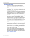
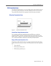
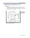
• To a lesser extent, PCB copper thickness (T) and proximity of same layer
ground plane.
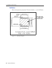
Figure 6.2 PCB Microstrip Topology
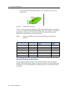
Table 6.1 shows typical track widths for an FR4 material PCB substrate (permittivity
ε
r
of 4.6 at 1.5 GHz) and different PCB thickness. One ounce copper is assumed for
the thickness of the top layer. If a Multi layer PCB is used, the thickness is the
distance from signal track to nearest ground plane.
Table 6.1 Typical Track Widths for an FR4 material PCB Substrate in Microstrip
Topology
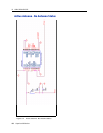
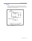
Microstrip Design Recommendations
It is recommended that the antenna connection PCB track be routed around the
outside of the module outline, kept on a single layer and have no bends greater than
45 degrees. It is not recommended, for production reasons, to route the track under
the module.
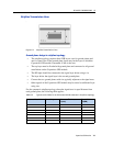
Substrate Material Permittivity Substrate Thickness
H (mm)
Track Width
W (MM)
1.6 2.91
1.2 2.12
1.0 1.81
FR4 4.6 0.8 1.44
0.6 1.07
0.4 0.71
0.2 0.34