


10 COPERNICUS REFERENCE BOARD
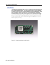
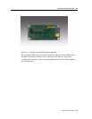
102 Copernicus GPS Receiver
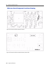
Reference Board I/O and Power Connector
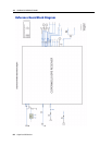
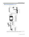
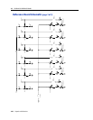
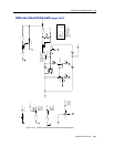
The Copernicus GPS reference board power and data I/O functions are integrated into
a single 8-pin header connector designated J7. The J7 connector uses 0.15 inch (3.8
mm) high pins on 0.0787 inch (2 mm) spacing. See the Copernicus GPS reference
board schematics, earlier in this chapter.
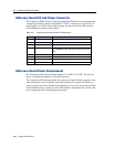
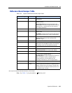
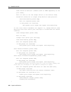
Table 10.1 Copernicus Reference Board Pin Description.
Reference Board Power Requirement
The Copernicus GPS reference board requires +3.0 VDC to 3.6 VDC. The receiver
power is supplied through pin 2 of the I/O connector.
The Copernicus GPS reference board also provides an input for back-up power used
when Copernicus is put in Standby mode and prime power is turned off. Back-up
power is used to keep the Copernicus RAM memory alive and to power the real-time
clock. RAM memory is used to store the GPS almanac, ephemeris, last position, and
user configuration data, including port parameters.
Pin # Function Description
1 TXD-B Port B transmit, CMOS/TTL
2 VCC 3.0 VDC to 3.6 VDC
3 TXD-A Port A transmit, CMOS/TTL
4 VBack 3.0 VDC to 3.3 VDC
The STANDBY supply shall be at least 0.3V less than
VCC.
5 RXD-A Port A receive, CMOS/TTL
6 1 PPS Pulse-Per-Second, CMOS/TTL
7 RXD-B Port B receive, CMOS/TTL
8 GND Ground, Power and Signal