


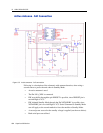

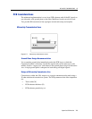


6 RF LAYOUT CONSIDERATIONS
72 Copernicus GPS Receiver
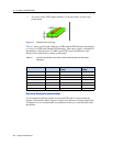
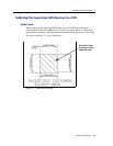
Design considerations for RF Track Topologies
The following items need to be considered for the Copernicus GPS Receiver RF
layout:
• PCB track connection to the RF antenna input must have impedance of 50
ohms.
• PCB track connection to the RF antenna input must be as short as possible.
• If an external antenna is used, PCB track connection to the RF antenna input
must transition from the circuit board to the external antenna cable, which is
typically a RF connector.
• If there are any ground planes on the same layer as the microstrip trace, please
refer to the Coplaner Waveguide design. Not covered in this manual.
• PCB track connection to the RF antenna input must be routed away from
potential noise sources such as oscillators, transmitters, digital circuits,
switching power supplies and other sources of noise.
• RF and bypass grounding must be direct to the ground plane through its own
low-inductance via
• Active or passive antennas may be used. If using a passive antenna the
connection to the antenna input shall be very short. It is possible to mount the
patch antenna on the same PCB as the Copernicus GPS module. Designers
must be aware of noise generating circuitry and proper design precautions
taken (shielding,.).
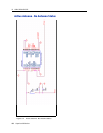
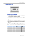
The PCB track connection to the RF antenna input must not have:
• Sharp bends.
• Components overlaying the track.
• Routing between components to avoid undesirable coupling.