


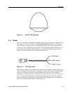
Lassen-SK8 Embedded GPS Module 2-3
Hardware Integration
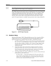
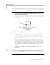
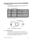
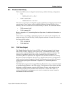
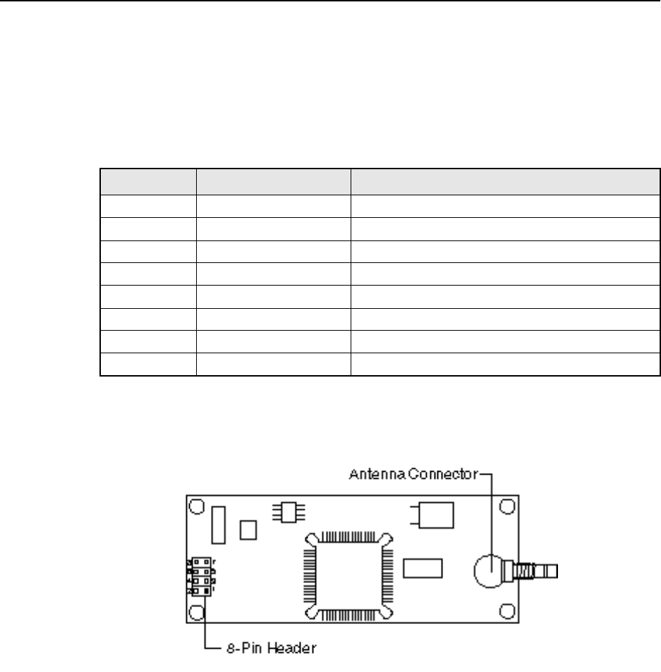
2.2 Interface Connector
The Lassen-SK8 power and data I/O functions are integrated into a single 8-pin header
connector, J4. The J4 connector uses 0.025 inch pins on 0.10 inch spacing (refer to the
mechanical outline drawing in Appendix F).
Pins 3 and 5 on J4 are also referred to as the primary serial port. Pins 1 and 7 are also
referred to as the secondary serial port.
Figure 2-3. Interface Connector Pin Identification
2.3 Power Requirement
The Lassen-SK8 receiver module requires +5 volts DC ±5% at 150 mA, typically
excluding the antenna. For power-on surge design considerations, the prime power should
be able to source up to a maximum load of 200 mA. The on-board capacitance on prime
power is 10 µF. An important design consideration for power is the receiver module's
internal clock frequency at 12.504 MHz ± 3 KHz. Interference spurs on prime power in
this narrow frequency band should be kept to less than 1mV.
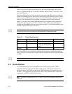
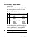
Table 2-1. I/O Connector Signals
Pin # Function Description
1 TXD 2 Port 2 transmit, CMOS/TTL
2 Prime Power 5VDC ±5%, 150 mA typical
3 TXD 1 Port 1 transmit, CMOS/TTL
4 Backup Power +3.2VDC to +5.25VDC, 2uA typical
5 RXD 1 Port 1 receive, CMOS/TTL
6 1 PPS Pulse-Per-Second, CMOS/TTL
7 RXD 2 Port 2 receive, CMOS/TTL
8 GND Ground, Power and Signal
7
5
3
1
5
8
5
4
2
6