


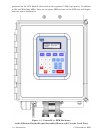

1-10 / Introduction CI-ControlWave EFM
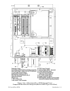
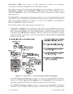
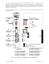
1.3.2.1 CPU Module Connectors
The CPU Modules contain up to seven connectors that function as follows (see Table 1-1):
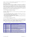
Table 1-1 - CPU Board Connector Summary
Ref. # Pins Function Notes
P1 76-Pin Factory Debug Not user accessible
P2 36-pin Card Edge Backplane I/O Bus Intf. see Figure 2-9
P3 44-pin Card Edge Backplane SCM Intf. see Figure 2-8
J2 10-Pin PLD JTAG Header Not user accessible
J3 9-pin COM1 9-pin male D-sub (RS-232) see Figure 2-11 & Table 2-3 or 4-2
J4 9-pin COM2 9-pin male D-sub (RS-232) see Figure 2-11 & Table 2-3 or 4-2
J5 9-pin COM3 9-pin male D-sub (RS-485) see Figure 2-11 & Table 2-3 or 4-2
CPU Module Comm. Port Connectors J3, J4 and J5
The CPU Module supports up to two external 9-pin RS-232 serial communication ports
(COM1 and COM2) and an external 9-pin RS-485 serial communication port (COM3).
COM1 and COM2 and COM3 utilize standard 9-pin male D-sub connectors. RS-232 ports
are protected with LCDA12C devices to ±4KV ESD. RS-485 port COM3 is protected with
LCDA12C and LCDA05 devices to ±4KV ESD.
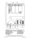
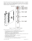
CPU Module I/OB Connector P2
CPU Module I/O Bus connector P2 provides a 36-pin interface between slot #2 (P3) of the
Backplane PCB and the CPU Module. Separate data, address and control buffers provide
access to the I/O bus which in turn provides up to 14 slots of memory mapped I/O Modules.
The CPU Module interface to the I/O Modules is through a set of buffers and transceivers
that are capable of driving up to fourteen I/O Modules.
CPU Module/System Controller Module Interface Connector (P3)
CPU Module/System Controller Module Interface connector (P3) provides a 44-pin interface
between slot #2 (P2) of the Backplane PCB and the CPU Module. The SCM provides:
- a wide input range Vin to 3.3V DC to DC Converter
- 1200 Millisecond good power detection
- Vin out of Spec. detection
- LED Status indication
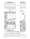
1.3.2.2 CPU Memory
Boot/downloader FLASH
Boot/download code is contained in a single 512Kbytes uniform sector FLASH IC. This
device resides on the local bus, operates at 3.3V and is configured for 8-bit access. 4-
Position DIP-Switch SW1’s position 3 allows start-up menu options to be displayed or boot-
up from system FLASH. If SW1-3 is closed when a reset occurs, the boot-up code will cause
a recovery menu to be sent out the COM1 serial port to a terminal program running on an
external host computer. Note: Recovery Mode will also be initiated if SCM Switch SW1
positions 1 and 2 are both set OPEN (Right) or CLOSED (Left) when a reset occurs.
FLASH Memory
The base version of the CPU Module has 8Mbytes of 3.3V, simultaneous read/write (DL)
FLASH memory. Each CPU Board contains two 48-pin TSOP sites that will each accept 4
or 8 Mbytes of 3.3V, (DL) FLASH IC, for a total of 4 or 8 Mbytes of memory. FLASH