Chapter 4 Functional Description
ATCA-C110/1G Installation and Use Manual
37
REVIEW COPY
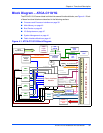
Block Diagram – ATCA-C110/1G
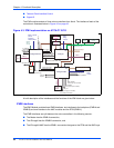
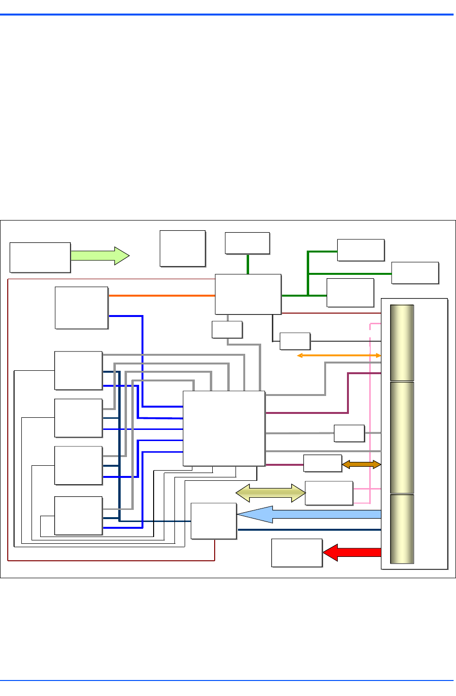
The ATCA-C110/1G server blade is divided into several functional blocks, see Figure 4-1. Each
of these functional blocks are described in the following sections:
■ Processor and Processor interfaces on page 38
■ Main Memory on page 40
■ Boot Device on page 40
■ I/O Subsystems on page 47
■ System Management on page 41
■ Fabric Interface Module on page 44
Figure 4-1. ATCA-C110/1G Block Diagram
x4 PCI-Express
x4 PCI-Express
x4 PCI-Express
x4 PCI-Express
x4 PCI-Express
1x XAUI
8x SerDes -Fabric interface
2x SerDes
Clock Signals
PCI 64bit, 66MHz
4x SerDes
DDR333 Interface
1x Serial
2x SerDes - Base
interface
1x XAUI
A
T
C
A
C
O
N
N
E
C
T
O
R
2x SATA
2x SATA
2x SATA
2x SATA
2x SerDes
2x SerDes
2x SerDes
Z
O
N
E
3
Z
O
N
E
2
Z
O
N
E
1
2x SerDes
JTAG Interface
Power
conversion
block
Telecom
Clocks Block
AMC
Slot 1
AMC
Slot 2
AMC
Slot 3
AMC
Slot 4
IPMC
Block
DDR
SDRAM
Update
Port
PCI-PCI-e
Bridge
PEX8114
BOOT
Flash
Fabric Interface
Module
Power QUICC III
TM
MPC8540
Processor
64/128MB
User
Flash
GPCM Interface
PHY
HARDWARE ADDRESS
Clock
Synthesizers
PHY
10/100
PHY
1X Serial
Recovery
Flash
Telecom Clocks
Glue
Logic
(CPLD)
1x 10/100 Ethernet


