


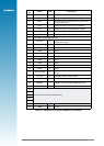
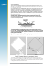
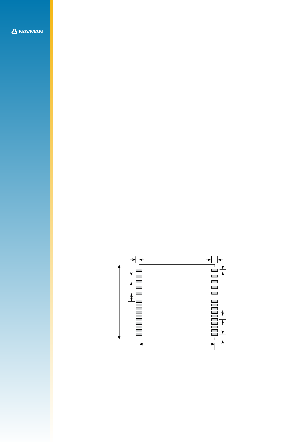
2.8
1.9
1.5
1.277
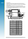
25.4 ±0.1
25.4 ±0.1
0.8
2.0
15
10
130
21
16
top view
of pad layout
(all measurements in mm)
1.0
Figure 2-3: Recommended application layout dimensions
LA000577C © 2006 Navman New Zealand. All rights reserved. Proprietary information and specications subject to change without notice.
9
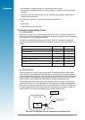
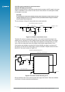
2.4.4 Serial RS232 data level shifter
To connect the module to a PC comm. port, the serial data signals must be level shifted to
RS232 levels. This has not been shown in the reference design, but many single chip RS232
level shifters are available, such as MAX3232.
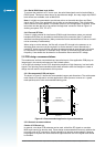
Note: It is highly recommended to provide test points on the serial data lines and ‘Boot’
signal (pad 3), even if the application circuit does not use these signals. This will allow the
user to connect to these signals if a rmware upload or new conguration is required. These
test points can take the form of an untted ‘through-hole’ connector. Refer to Figure 2-2
showing test points TPO, TPI & TP.
2.4.5 External RF lter
If there is a high potential for interference (EMI) though the antenna system, an external
bandpass SAW lter may be added to the antenna input connection (pad 17) which will
attenuate interfering frequencies. (Many commercial active antennas have a lter so it would
not be necessary to add another).
When using an active antenna, the lter will not pass DC through to the antenna, so an
alternate power source would be required if an active antenna is used. Alternatively a
parallel RF choke across the lter will allow the antenna power to pass through, but choice
of components is important, for example using a choke of sufciently high self-resonant
frequency. Care should also be taken not to exceed the lter maximum DC voltage.
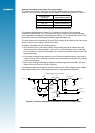
2.5 PCB design recommendations
The modules are surface mounted devices, hence the layout of the application PCB plays an
integral part in the overall performance of the nished system.
It is not difcult to design such a PCB, despite the presence of high frequency, low level radio
signals. The following recommendations have been offered to allow the designer to create a
design that will meet the requirements of this product.
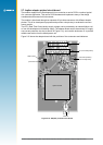
2.5.1 Recommended PCB pad layout
The layout in Figure 2-3 shows the recommended copper pad dimensions. The solder paste
mask needs to be adjusted to suit the application’s reow process, however a 1:1 (paste
mask:pad size) ratio is the recommended starting point.
2.5.2 General recommendations
Choice of PCB stack up
In general, a two layer PCB substrate can be used, with all the RF signals on one side.
Multi-layer boards can also be used. These design recommendations here only address the
microstrip style of RF connection. Stripline designs can also be accommodated. However,
long lengths of stripline can cause excessive signal loss and vias in the signal track should
be avoided.