


LA000577C © 2006 Navman New Zealand. All rights reserved. Proprietary information and specications subject to change without notice.
16
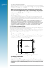
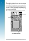
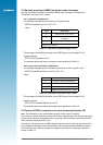
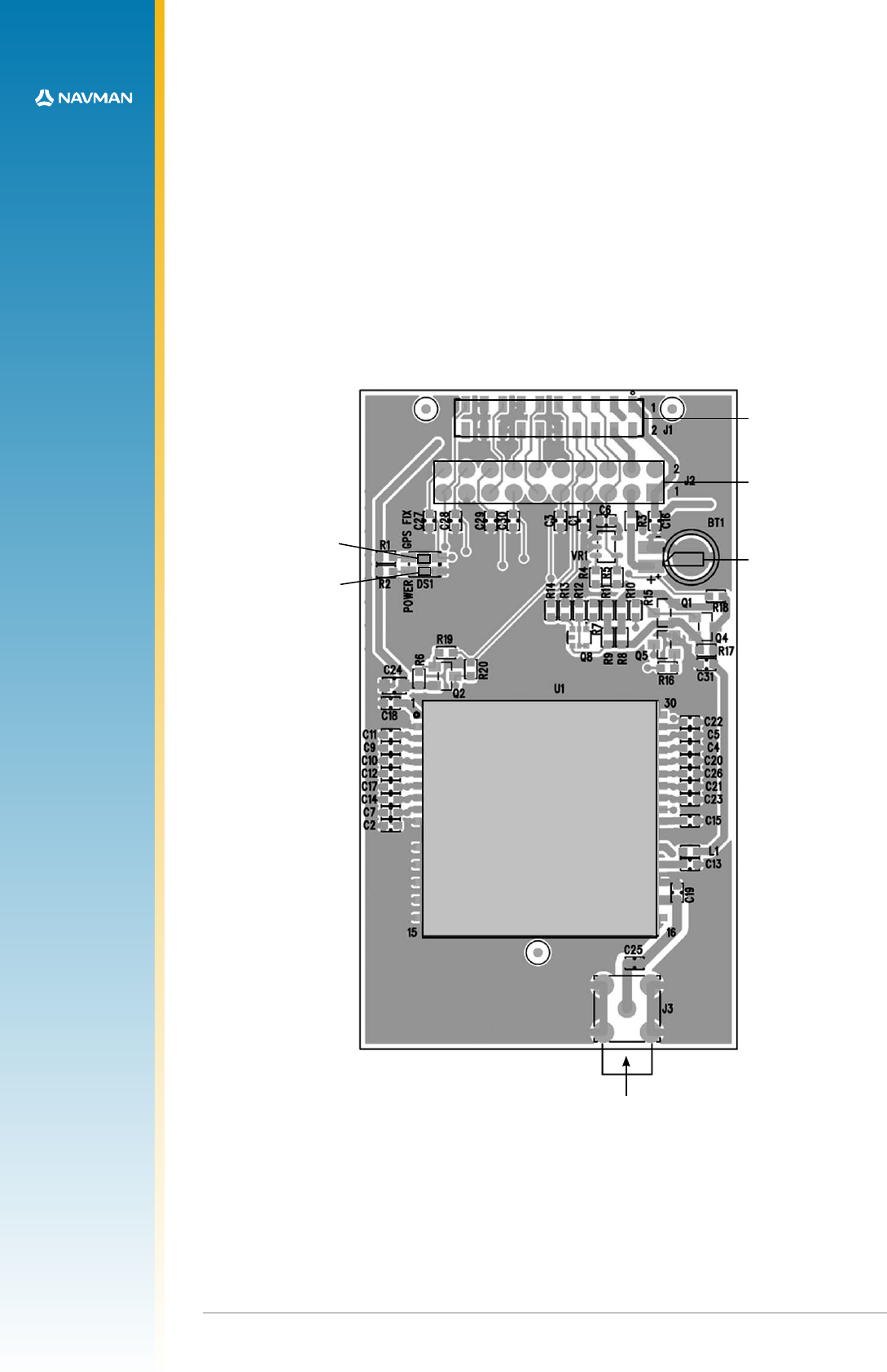
2.7 Jupiter adapter printed circuit board
The module supplied in the Development kit is mounted on a carrier PCB in a method typical
of a customer application. This carrier PCB illustrates and implements many of the design
considerations discussed in this document.
The module is interfaced through two separate 20-pin data connectors with different header
pitches. This is for development purposes and provides a simple way to evaluate the surface
mount module.
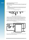
The RTC (Real-Time Clock) backup supply voltage can be provided by an onboard lithium cell,
or from the development unit backup supply. The adapter board carries the antenna DC supply
over-current protection circuits (as shown in Figure 2-11), and a switch de-bounce IC to provide
reliable reset action from the development unit.
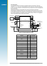
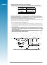
Figure 2-12 shows the adapter board with the positions of the connectors and indicators.
Jupiter module
antenna
power LED
GPS x LED
J1
J2 (not normally tted)
RTC backup battery
(not normally tted)
Figure 2-12: Adapter printed circuit board