


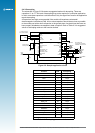
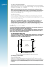
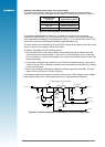
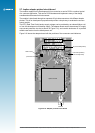
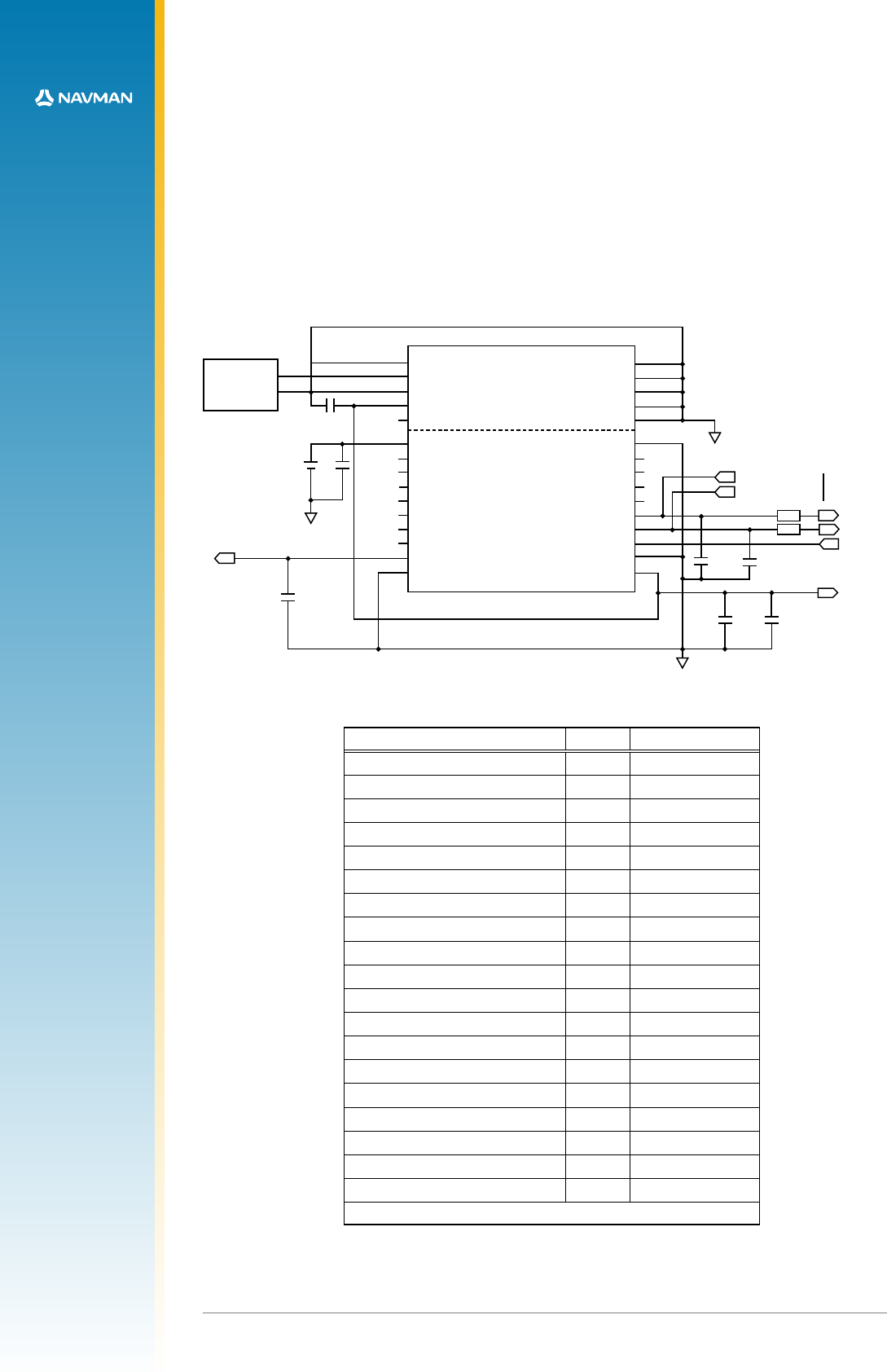
Figure 2-2: Sample application circuit
Jupiter 30 or Jupiter 20 GPS Module
16
17
18
19
20
21
22
23
24
25
26
27
28
29
30
J1 coaxial connector
MCX, SMA or MMCX
GND
1PPS
C4
27pF
C3
1nF
3 V RTC lithium
backup battery
1nF
C7
GND
I/P
1
2
DGND
15
14
13
12
11
10
9
8
7
6
5
4
3
2
1
AGND
C2
10nF
C1
1µF
POWER
C5
27pF
C6
27pF
TP
TPO
TPI
SDI
SDO
R1
R2
10K
10K
serial data ports
to application processor
or RS232 level converter
GND
RF_IN
GND
V_ANT
VCC_RF
V_BATT
RESET
GPIO/GPS_FIX
GPIO
GPIO
GPIO/WAKE_UP
GPIO/ANT_OC
GPIO/ANT_CTRL
GPIO/1PPS
GND
GND
GND
GND
GND
GND
GND
RF_ON
RXB
TXB
TXA
RXA
BOOT
GND
PWRIN
GPIO/NANT_SC
RF
Digital
LA000577C © 2006 Navman New Zealand. All rights reserved. Proprietary information and specications subject to change without notice.
8
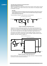
2.4.3 Decoupling
The schematic in Figure 2-2 illustrates a suggested method of decoupling. These are
capacitors C1 to C7. This level of decoupling may not be required in a particular application,
in which case these capacitors could be omitted. Only the signal lines used in the application
require decoupling.
All capacitors are highly recommended if the module will experience substantial
electromagnetic interference (EMI). All low value capacitors should be as close as possible
to the module pad with a short connection to the ground plane. Any data lines that have not
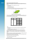
been properly shielded are susceptible to data corruption. Refer to Table 2-3 for suggested
values of decoupling relative to the function desired.
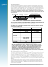
Function Pad Decoupling
PWRIN 1 1 µF||1 nF
BOOT 3 27 pF
RXA 4 27 pF
TXA 5 27 pF
TXB 6 27 pF
RXB 7 27 pF
NANT_SC 8 27 pF
RF_ON 9 27 pF
ACTIVE_PWR 19 1 nF
VCC_RF 20 1 nF
V_BATT 21 1 µF||1 nF
NRESET 22 27 pF
GPS_FIX 23 27 pF
GPIO13 24 27 pF
GPIO4 25 27 pF
WAKEUP 26 27 pF
ANT_OC 27 27 pF
ANT_CTRL 28 27 pF
1PPS 29 27 pF
Note: ‘||’ represents a parallel connection
Table 2-3: Decoupling recommendations