


LA000577C © 2006 Navman New Zealand. All rights reserved. Proprietary information and specications subject to change without notice.
Figures
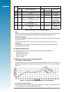
Figure 2-1: Lead-free and tin/lead reow prole recommendation ..................................... 6
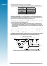
Figure 2-2: Sample application circuit ................................................................................ 8
Figure 2-3: Recommended application layout dimensions................................................. 9
Figure 2-4: Typical module layout .....................................................................................10
Figure 2-5: Example PCB layout for external active antenna ............................................10
Figure 2-6: PCB microstrip dimensions .............................................................................11
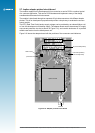
Figure 2-7: Arrangement of active antenna and application board....................................12
Figure 2-8: Cross section of application board with passive patch antenna .....................13
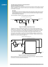
Figure 2-9: Simple current limiter circuit ............................................................................14
Figure 2-10: Active current limit using an IC ......................................................................14
Figure 2-11: Antenna short/open circuit sensor circuit (3.3 V supply only)
........................15
Tables
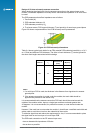
Table 2-1: Jupiter 30 and Jupiter 20 Module pin functions ................................................. 5
Table 2-2: Summary of pin multi-functionality .................................................................... 6
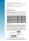
Table 2-3: Decoupling recommendations ........................................................................... 8
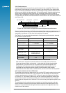
Table 2-4: PCB substrate thicknesses v track width .........................................................11
Table 2-5: Passive and active antenna features ................................................................12
Table 2-6: Recommended antenna characteristics ...........................................................13
Table 2-7: Antenna sense and control functions ...............................................................15
Table 2-8: Connector conguration ...................................................................................17
Table 3-1: Low power modes message values ................................................................ 20
Table 3-2: Low power acquisition input values ................................................................. 20
Table 3-3: Pin conguration of the GPIO lines ..................................................................21
Table 3-4: Antenna status output message values .......................................................... 22