


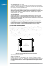
LA000577C © 2006 Navman New Zealand. All rights reserved. Proprietary information and specications subject to change without notice.
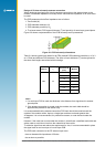
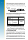
5
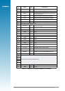
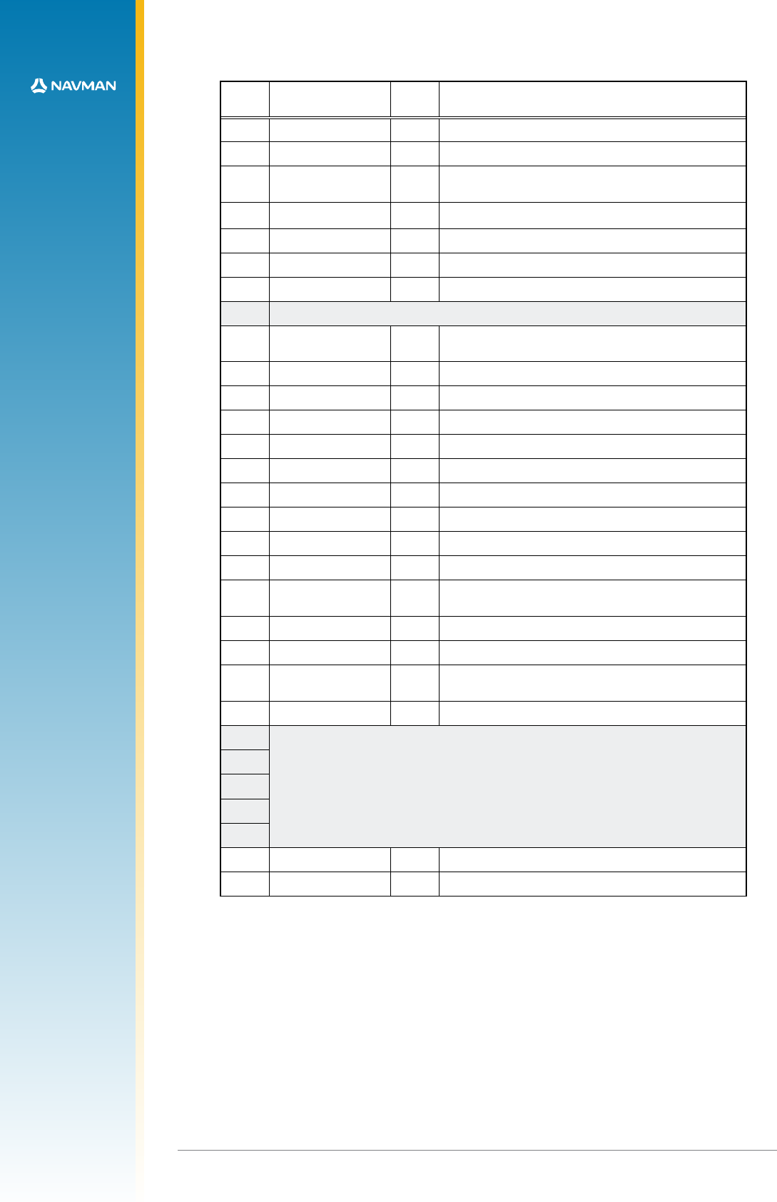
Pin
No.
Name Type Description
1 PWRIN P main power input (3.3 V)
2 GND P ground
3 BOOT I
serial boot (high for serial boot, low or open circuit
for normal operation)
4 RXA I CMOS level asynchronous input for UART A
5 TXA O CMOS level asynchronous output for UART A
6 TXB O CMOS level asynchronous output for UART B
7 RXB I CMOS level asynchronous input for UART B
8 pin 8 multi-functional (see table 2-2)
9 RF_ON O
output to indicate whether the RF section is
enabled (active high)
10 GND P ground
11 GND P ground
12 GND P ground
13 GND P ground
14 GND P ground
15 GND P ground
16 GND P ground
17
RF_IN I RF input
18 GND P ground
19 ACTIVE_PWR P
active power input, 70 mA current limit supply to
this pin
20 VCC_RF O RF Power (+2.85 V) supply output
21 V_BATT P backup battery input
22 NRESET I
external reset (active low), voltage on PIN 22
NRESET must not exceed PWRIN at all times
23 GPS_FIX O GPS x indication (active low)
24
pins 24-28 multi-functional (see table 2-2)
25
26
27
28
29 1PPS O 1 pulse per second output
30 GND P ground
Table 2-1: Jupiter 30 and Jupiter 20 Module pin functions