


190-00067-25 Rev D 1-5
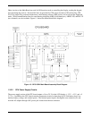
External battery pack power is also applied to the rear connector (J1). All of these sources are diode isolated to
prevent parallel sourcing. The unit is turned on and off by a digital latch circuit operated by a knob located on
the front panel adjacent to the data card opening. The switching circuit is a fly-back design and operates at a
frequency of approximately 128 kHz. The +15 V output is post regulated to provide 11.75 to 12.25-V. The +5 V
output is regulated at 4.8-V. All other voltages are ±20%.
1.3.3 GPS Receiver
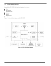
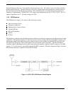
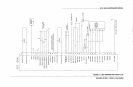
The GPS Receiver (Figure 1-4) consists of the following circuitry:
Dual conversion receiver
Frequency synthesizer
High precision crystal oscillator
Ceramic RF filter
RF and IF amplifiers
Mixers
IF filter
The frequency synthesizer uses the high-precision oscillator as a reference frequency for the phase detector in the
synthesizer. The resultant frequency is used in the mixer section to product the first intermediate frequency (IF).
After further amplification and mixing with a product of the crystal oscillator, the baseband IF is passed to the
CPU Board for processing. The crystal output is also used for the system clock pulse. The GPS assembly is
contained within a shielding fence/cover and connection to the antenna is made via a BNC connector. The GPS
supplies +5 V to the antenna’s preamplifier through this BNC connector. The block diagram in Figure 1-4 shows
the interaction between components on the GPS Assembly.
Figure 1-4. GPS 155XL GPS Receiver Block Diagram