


LA000605D © 2007 Navman New Zealand. All rights reserved. Proprietary information and specications subject to change without notice.
6
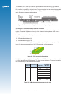
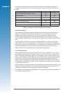
2.3.3 Decoupling components
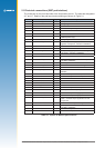
The recommended values for power and signal decoupling are shown in Table 2-2. The
placement of these components must ensure that the low value capacitors have very short
connections to the module pad and to the ground plane.
Function Pad Decoupling
PWRIN F1 1 µF||10 nF
BOOT C4 27 pF
RXA D5 27 pF
TXA D7 27 pF
TXB F6 27 pF
RXB E6 27 pF
RF_ON A7 27 pF
VANT A4 1 nF
VCC_RF F3 1 µF||1 nF
VBATT F2 10 nF
N_RESET E5 27 pF
N_GPS_FIX D4 27 pF
GPIO (ALL) - 27 pF
WAKEUP F4 27 pF
LNA_EN C5 27pF
1PPS E7 27 pF
Note: ‘||’ represents a parallel connection
Table 2-2: Decoupling recommendations
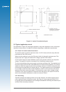
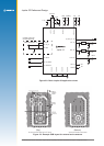
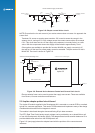
2.3.4 Antenna connection
The PCB layout design of the antenna input connection requires the appropriate selection of
PCB track width, substrate material and careful attention to the layout geometry. If this overall
system is not implemented correctly, the module will receive poor GPS signals and therefore
provide inferior navigation data.
Figure 2-5 shows an example of a PCB design integrating an external active antenna
connected via an MCX or SMA coaxial connector.
Application PCB
Jupiter
module
Active GPS
antenna
connecting coax carrying
GPS signals and DC
power for amplication
coaxial connector
tted to application
PCB
Figure 2-5: Arrangement of active antenna and application board